Photopatternable molecular circuitry

a molecular circuit and molecular technology, applied in the field of photopatternable molecular circuitry, can solve the problems of adversely altering the properties of the ultra-thin junction, essentially unremovable/inseparable, barrier materials between the molecule and the conventional resist, etc., to reduce or eliminate the conventional photoresist masking layer, simplify the traditional process, and reduce the effect of tim

Inactive Publication Date: 2003-10-16
HEWLETT PACKARD DEV CO LP
View PDF13 Cites 27 Cited by
  • Summary
  • Abstract
  • Description
  • Claims
  • Application Information

AI Technical Summary

Benefits of technology

[0017] An advantage of the present invention over the prior art is that the top electrode (the second set of electrodes) does not define the junction. Rather, the molecular area is defined independently, due to the use of the photosensitive group.
[0018] The present invention provides a class of bistable molecular switches with at least one photosensitive functional group on the molecule. Those molecules can serve as both a molecular device and photoresist-type mask for patterning a layer to fabricate molecular circuits. This will simplify the traditional process and shorten the time to produce a batch of circuits, leading to inexpensive products, such as electronic memory (write once or rewriteable), electronically addressable displays, and generally any circuit for which organic electronics or opto-electronics will be acceptable.
[0019] Advantageously, the present invention reduces or eliminates conventional photoresist masking layers, and simplifies the fabrication of micro-scale and nano-scale circuits.
[0020] FIG. 1 is a perspective elevational view, schematically depicting two crossed wires, with at least one molecule at the intersection of the two wires;
[0021] FIGS. 2a-2f provide a schematic representation of the prior art steps that use lithographically deposited (micrometer or sub-micrometer scale diameter) wires;
[0022] FIGS. 3a-3d depict a schematic representation of process steps in accordance with the present invention for producing photo-patternable molecular circuitry;

Problems solved by technology

Making and using resist by conventional means (especially in direct contact with the molecule, or connector species) could adversely alter the properties of the ultra-thin junction.
Further, barrier materials between the molecule and the conventional resist could adversely alter the properties of the junction itself; for example, many metallic species could diffuse into or bind tightly with the molecule, becoming essentially unremovable / inseparable.
Polymer electronics on this thickness scale (nanometers) presents special problems (rotaxane studies by Collier et al, supra, are on the order of 100 .ANG. or less).

Method used


Image

  • Photopatternable molecular circuitry
  • Photopatternable molecular circuitry
  • Photopatternable molecular circuitry

Examples


example 1b

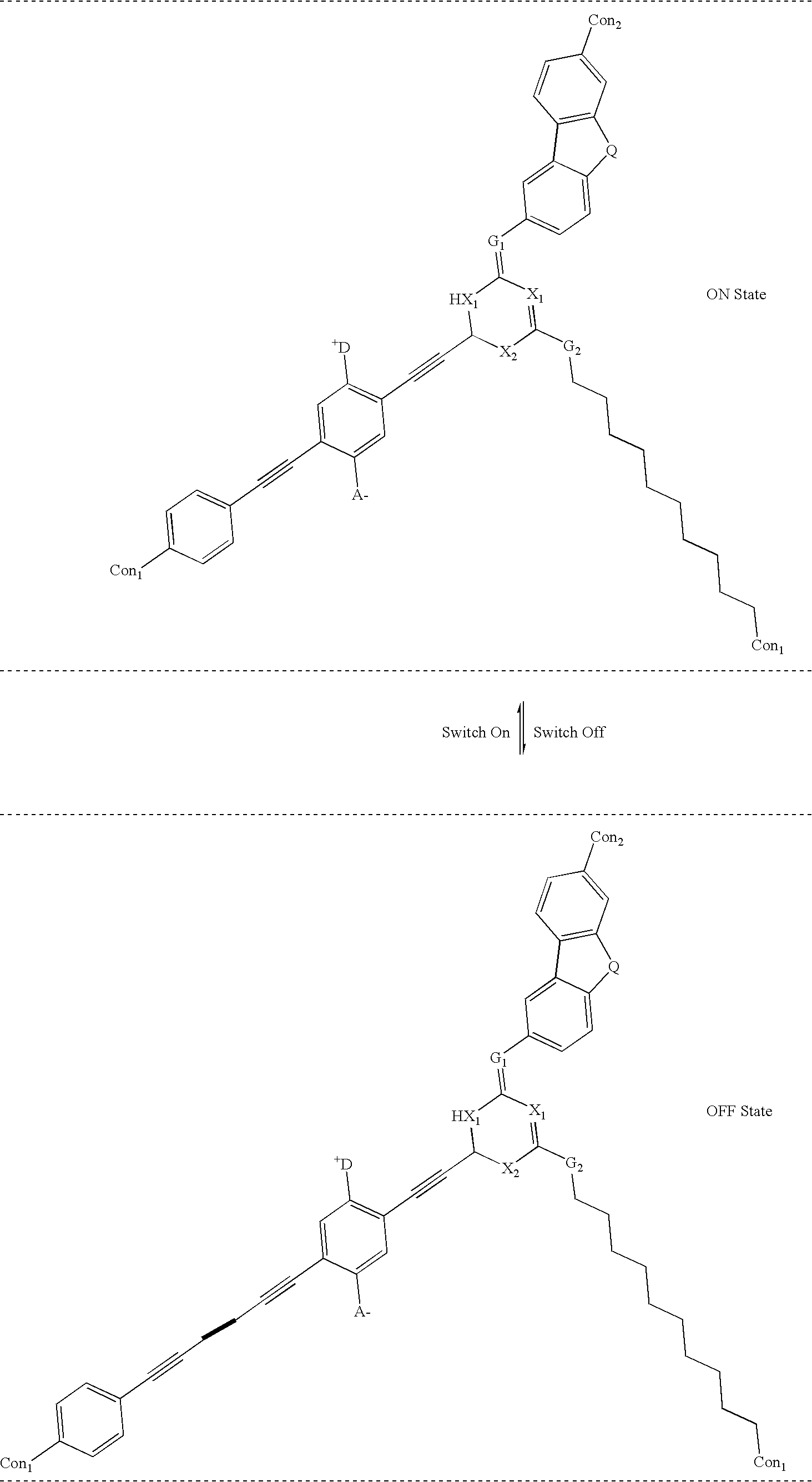
[0087] Example 1b below is a real molecular example of one embodiment of the present invention, which relies on a rotor portion combined with a stator portion. In Example 1b, the rotation axis of the rotor is designed to be in a 30 to 70 degree angle to the net current-carrying axis of the molecules. 1

[0088] where:

[0089] The symbol A.sup.-is an Acceptor group; it is an electron-withdrawing group. It may be one of following: carboxylic acid or its derivatives, sulfuric acid or its derivatives, phosphoric acid or its derivatives, nitro, nitrile, hetero atoms (e.g., N, O, S, P, F, Cl, Br), functional group with at least one of above-mentioned hetero atoms (e.g., OH, SH, NH, etc.), hydrocarbons (either saturated or unsaturated), or substituted hydrocarbons.

[0090] The symbol D.sup.+ represents a Donor group; it is an electron-donating group. It may be one of following: hydrogen, amine, OH, SH, ether, hydrocarbon (either saturated or unsaturated), substituted hydrocarbon, or a functional ...

example 2b

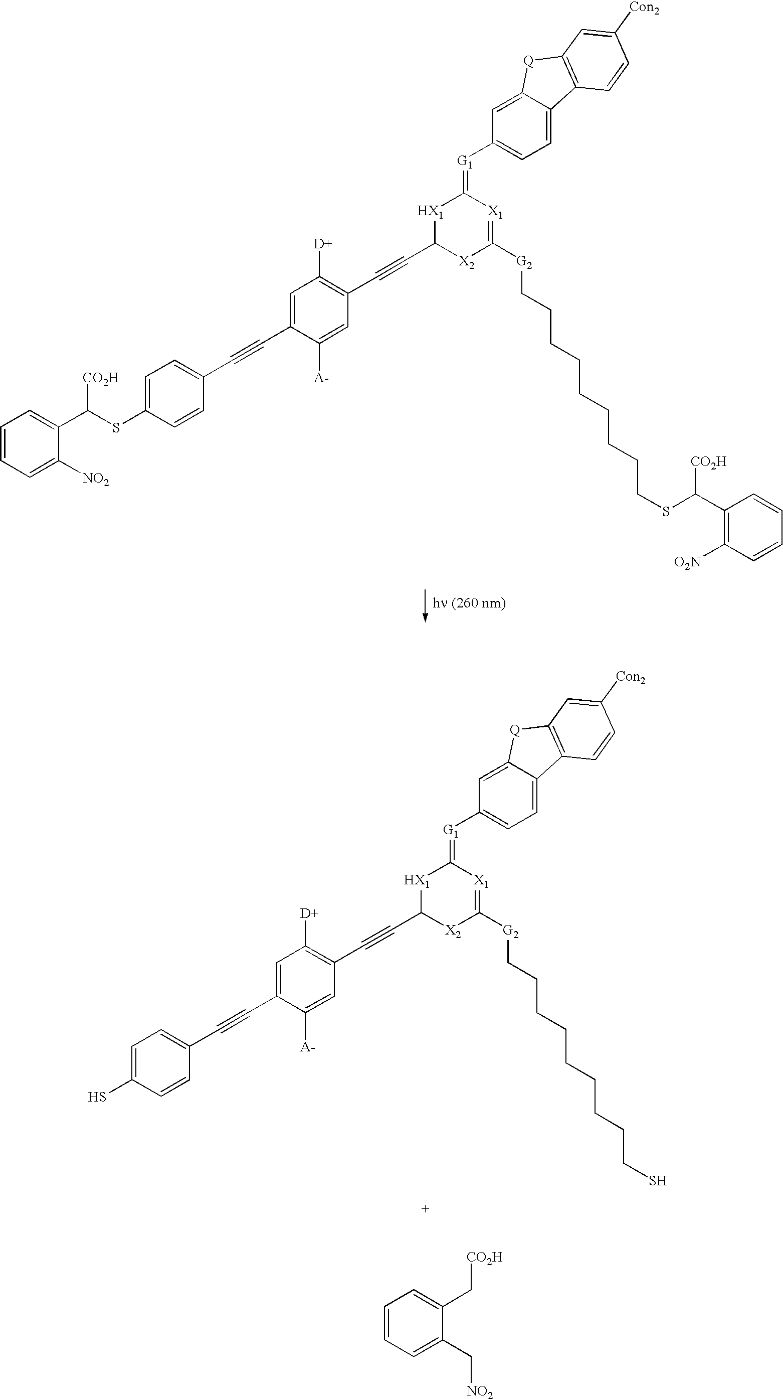
[0130] Example 2b below shows a real example of a PSG-modified switchable molecule, which contains PSGs on both the connecting units and the bridging groups Upon UV irradiation, both connecting groups and bridging groups decompose to form small molecules, which are removable by base and / or solvent washing. 4

[0131] where:

[0132] The symbol A.sup.- is an Acceptor group; it is an electron-withdrawing group. It may be one of following: hydrogen, carboxylic acid or its derivatives, sulfuric acid or its derivatives, phosphoric acid and its derivatives, nitro, nitrile, hetero atoms (e.g., N, O, S, P, F Cl, Br), or a functional group with at least one of above-mentioned hetero atoms (e.g., OH, SH, NH, etc.), hydrocarbon (either saturated or unsaturated), or substituted hydrocarbon.

[0133] The symbol D.sup.+ represents a Donor group; it is an electron-donating group. It may be one of following: hydrogen, amine, OH, SH, ether, hydrocarbon (either saturated or unsaturated), substituted hydrocarb...
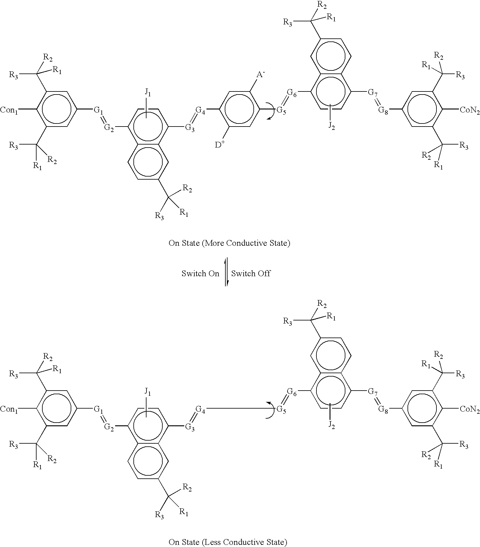
example 4b

INDUSTRIAL APPLICABILITY

[0153] The use of a molecular photoresist as described herein is expected to find use in the fabrication of micrometer-scale and nanometer-scale devices.


PUM

PropertyMeasurementUnit
thicknessaaaaaaaaaa
sizeaaaaaaaaaa
thickaaaaaaaaaa

Abstract

Bistable molecules are provided with at least one photosensitive functional group. As thus constituted, the bistable molecules are photopatternable, thereby allowing fabrication of micrometer-scale and nanometer-scale circuits in discrete areas without relying on a top conductor as a mask. The bistable molecules may comprise molecules that undergo redox reactions, such as rotaxanes and catenanes, or may comprise molecules that undergo an electric-field-induced band gap change that causes the molecules, or a portion thereof, to rotate, bend, twist, or otherwise change from a substantially fully conjugated state to a less conjugated state. The change in states in the latter case results in a change in electrical conductivity.

Description

[0001] The present invention relates generally to methods of making electronic circuitry, and, more particularly, to forming the elements of the electronic circuitry directly, without the need for separate photoresist steps.[0002] Photoresist masks for patterning layers to fabricate electronic circuits are well-known. That technology is the basis for today's microcircuits. Briefly, positive or negative polymeric resists are used, involving the formation of a layer of resist on a surface, exposing the resist to radiation (visible, UV, X-ray, etc.) through a mask to cross-link (or unlink) portions of the resist, followed by removal of unwanted portions of the resist. The resist then serves as a mask for further processing steps, such as ion implantation, oxidation, metallization, and the like.[0003] The area of molecular electronics is in its infancy. Developments in nanotechnology (critical dimension measured in nanometers) are directed to new generations of electronic circuitry, hav...

Claims


Application Information

Patent Timeline
Patent Type & Authority Applications(United States)
IPC IPC(8): G03F7/004G11C11/56G11C13/02G11C13/04H01L27/28H01L51/30H01L51/42
CPCB82Y10/00G03F7/0045G11C11/5664G11C13/0014G11C13/02G11C13/04H01L51/42G11C2213/77G11C2213/81H01L27/285H01L51/005H01L51/0052H01L51/0595G11C13/048H10K19/202H10K85/60H10K85/615H10K10/701H10K30/00
Inventor BECK, PATRICIA A.ZHANG, XIAO-ANZHOU, ZHANG-LIN
Owner HEWLETT PACKARD DEV CO LP
Why Eureka
Try Eureka