Method for forming transistor of semiconductor device

a semiconductor device and transistor technology, applied in the direction of transistors, semiconductor devices, electrical appliances, etc., can solve the problems of less than 30 nm channel depth, inability to detect the presence of dopants in the channel, and the surface roughness of the substrate is aggravating, so as to achieve the effect of high integration density of the semiconductor devi

Inactive Publication Date: 2003-11-20
SK HYNIX INC
View PDF0 Cites 113 Cited by
  • Summary
  • Abstract
  • Description
  • Claims
  • Application Information

AI Technical Summary

Benefits of technology

0014] Accordingly, a method for forming a transistor of a semiconductor device is disclosed which provides high integration density of the semiconductor device by controlling loss of dopants during thermal process and diffusion of dopant during SEG In order to achieve the above-described object of the invention, a method for forming a transistor of a semiconductor device is disclosed which comprises: (a) defining a first and a second regions on a semiconductor substrate using a device isolation pattern; (b) ion-implanting a first conductive type impurity into the first region to form a first channel layer; (c) ion-implanting a second conductive type impurity into the second region, using exposure mask to form a second channel layer; (d) performing high temperature thermal process to stabilize the first and second channel layers; (e) performing a hydrogen treatment process on the structure resulting from step (d); (f) growing undoped silicon epitaxial layers on the first and the second channel layers of the first conductive type and the stabilized channel layer whereby generating a first and a second .delta.-doped epitaxial channels of a super-steep-retrograde structure; (g) forming a gate insulating film and a gate electrode on the first and the second .delta.-doped epitaxial channels, respectively; (h) re-oxidizing the gate insulating film to repair damaged portions of the gate insulating film; and (i) forming a source / drain region and performing a low temperature thermal process.

Problems solved by technology

However, since loss and diffusion of channel dopants during an epitaxial channel formation and subsequent thermal process are difficult to control, conventional epitaxial channel transistors fail to provide an improved Ion / Ioff characteristics.
However, an embodiment of a .delta.-doped epitaxial channel having a channel depth of less than 30 nm has not been reported to be possible diffusion of dopants in the subsequent process even when a doped epitaxial layer and an undoped epitaxial layer are employed.
However, the laser thermal process, which controls loss and diffusion of dopants to the epitaxial layer, generates partial melting on a silicon substrate under the laser power, resulting in an aggravation of surface roughness of the substrate and a generation of crystal defect, and cannot be applied to a practical method for manufacturing a semiconductor device.

Method used


Image

  • Method for forming transistor of semiconductor device
  • Method for forming transistor of semiconductor device
  • Method for forming transistor of semiconductor device

Examples


Embodiment Construction

[0021] Preferred methods for forming a transistor of a semiconductor device will now be described in detail with reference to the accompanying drawings.

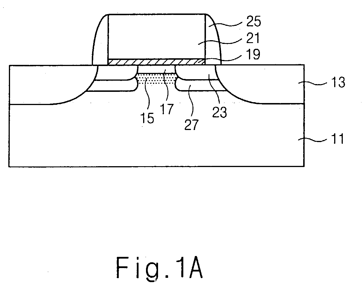
[0022] FIG. 1a is a schematic cross-sectional diagram illustrating a transistor having an ultra-shallow super-steep-retrograde (SSR) silicon epitaxial (Si-Epi) channel. Referring to FIG. 1a, the transistor comprises a semiconductor substrate 11, a stacked structure of a gate insulating film 19 and a gate electrode 21 disposed on the semiconductor substrate 11, an insulating film spacer 25 disposed on the sidewalls of the stacked structure, a source / drain region 13 and a source / drain extension region 23 disposed on the semiconductor substrate 11 at both sides of the stacked structure, a punch stop 27 disposed below the source / drain extension region 23, a channel layer 15 disposed between the source / drain extension regions 23, and an epitaxial channel layer 17 disposed on the channel layer 15 under the gate insulating film 19. Here, a ...


PUM

PropertyMeasurementUnit
depthaaaaaaaaaa
energyaaaaaaaaaa
temperatureaaaaaaaaaa

Abstract

A method for forming a transistor of a semiconductor device, including the step of forming a channel layers of a first and a second conductive types, performing high temperature thermal process to form stabilized channel layers and forming an epitaxial channel structure having a super-steep-retrograde delta-doped layer by growing undoped silicon epitaxial layers, treating the entire surface of the resulting structure with hydrogen, forming an epitaxial channel structure by growing undoped silicon epitaxial layers on the stabilized channel layers, forming gate insulating films and gate electrodes on the epitaxial channel structures, re-oxidizing the gate insulating films for repairing damaged portions of the gate insulating films; and forming a source/drain region and performing a low temperature thermal process.

Description

[0001] 1. Technical Field[0002] A method for forming a transistor of a semiconductor device is disclosed and, in particular, an improved method for forming a metal-oxide-semiconductor field effect transistor (MOSFET) or metal-insulator-semiconductor field effect transistor (MISFET) is disclosed which has an ultra-shallow super-steep-retrograde epitaxial channel with a channel length below 100 nm that can be applied to an ultra large scale integrated (ULSI) semiconductor device.[0003] 2. Description of the Related Art[0004] A surface region below a gate electrode and a gate insulating film of a MOSFET or MISFET semiconductor device serves as a current path when an electric field is applied to a source / drain region with a voltage applied to a gate. This region is called a channel.[0005] The characteristics of the MOSFET or MISFET semiconductor device are determined by a dopant concentration in the channel region. Specifically, the characteristics of the device such as a threshold volt...

Claims


Application Information

Patent Timeline
Patent Type & Authority Applications(United States)
IPC IPC(8): H01L27/092H01L21/28H01L21/336H01L21/8238H01L29/10H01L29/36H01L29/78
CPCH01L21/28185H01L21/28202H01L29/66651H01L29/105H01L29/365H01L21/823807H01L21/18
Inventor SOHN, YONG SUNRYOO, CHANG WOOLEE, JEONG YOUB
Owner SK HYNIX INC
Why Eureka
Try Eureka