Method for producing boride thin films

a thin film and boride technology, applied in the direction of superconductor devices, crystal growth process, polycrystalline material growth, etc., can solve the problems of inability to achieve inability to meet most electronic applications, and inability to achieve reproducible hts josephson junctions with sufficiently small variations in device parameters. achieve high critical temperature, low roughness, and high purity

Inactive Publication Date: 2003-11-27
PENN STATE RES FOUND
View PDF7 Cites 14 Cited by
  • Summary
  • Abstract
  • Description
  • Claims
  • Application Information

AI Technical Summary

Benefits of technology

0013] Another aspect of the present invention is a thin film suitable for use in semiconductor applications. In an embodiment of the pre

Problems solved by technology

However, the Nb-based circuits must operate at temperatures close to 4.2 Kelvin (K), which requires heavy cryocoolers with several kilowatts of input power, which is not acceptable for most electronic applications.
Circuits based on high temperature superconductors (HTS) would advance the field, but 17 years after their discovery, reproducible HTS Josephson junctions with sufficiently small variations in device parameters have proved elusive.
The su

Method used


Image

  • Method for producing boride thin films
  • Method for producing boride thin films
  • Method for producing boride thin films

Examples


Embodiment Construction

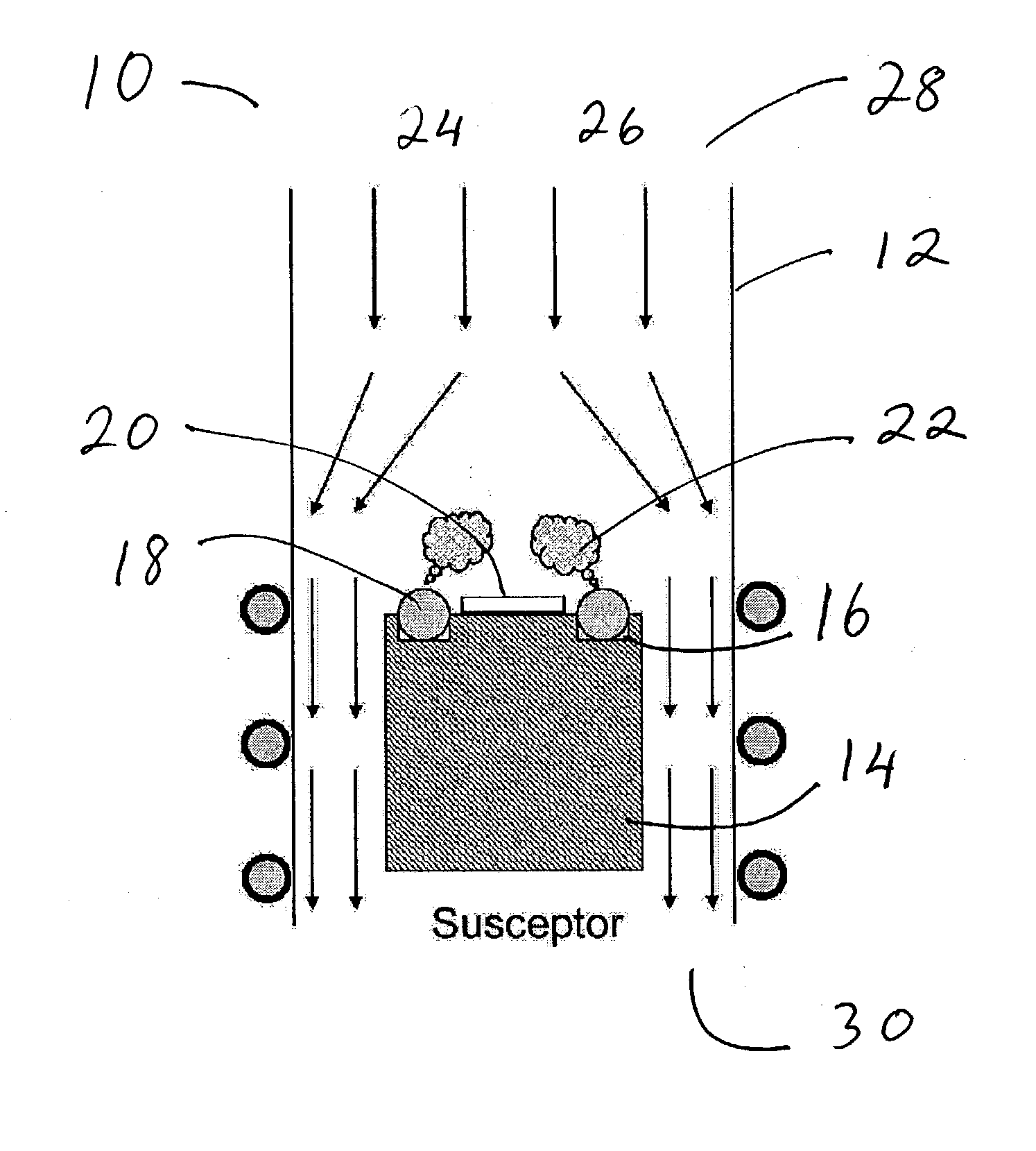
[0022] The present invention contemplates forming thin films by combining the techniques, in part, of a physical vapor deposition (PVD) process with that of a chemical vapor deposition (CVD) process. This hybrid physical chemical vapor deposition (HPCVD) process addresses various problems arising in fabricating thin films of superconducting materials, which often need high purity and morphological integrity for efficient superconducting properties and which are not readily achieved by either PVD or CVD individually.

[0023] Although the present invention is suited for depositing superconducting materials, other thin film materials are also contemplated. The present methods can achieve forming high purity films by reducing or eliminating the need for organometallic compounds, as is typically used in CVD or metalorganic CVD (MOCVD). The metal or metal source is provided by physically generating vapor from a source material, such as practiced with PVD. A separate precursor is combined wi...


PUM

PropertyMeasurementUnit
Temperatureaaaaaaaaaa
Pressureaaaaaaaaaa
Pressureaaaaaaaaaa

Abstract

Thin films of conducting and superconducting materials are formed by a process which combines physical vapor deposition with chemical vapor deposition. Embodiments include forming boride films, such as magnesium diboride, in high purity with superconducting properties on substrates typically used in the semiconductor industry by physically generating magnesium vapor in a deposition chamber and introducing a boron containing precursor into the chamber which combines with the magnesium vapor to form a thin boride film on the substrate.

Description

[0001] The present application claims priority to U.S. Provisional Application Serial No. 60 / 367,815 filed Mar. 25, 2002 and entitled "HYBRID PHYSICAL-CHEMICAL VAPOR DEPOSITION OF MAGNESUM DIBORIDE AND OTHER BORIDE FILMS", the entire disclosure of which is hereby incorporated in its entirety herein by reference.[0002] The present invention relates to boride thin films and methods of their formation and, in particular, to magnesium diboride thin films for use in superconducting electronics such as superconducting integrated circuits, in coated-conductor tapes, and other applications using superconductor thin films.[0003] Integrated circuits using superconductors are more suitable for ultrafast processing of digital information than semiconductor-based circuits. Niobium (Nb) based superconductor integrated circuits using rapid single flux quantum (RSFQ) logic have demonstrated the potential to operate at clock frequencies beyond 700 GHz. However, the Nb-based circuits must operate at ...

Claims


Application Information

Patent Timeline
IPC IPC(8): C23C14/00C23C14/06C30B23/02H01L29/78H01L39/24
CPCC23C14/0021C23C14/0057C23C14/067C30B23/02Y10T29/49014H01L39/2487H01L39/2493H01L29/7834C30B29/10H10N60/0856H10N60/0912
Inventor ZENG, XIANGHUIPOGREBNYAKOV, ALEXEJXI, XIAOXINGREDWING, JOAN M.LIU, ZI-KUISCHLOM, D. G.
Owner PENN STATE RES FOUND
Why Eureka
Try Eureka