Sacrificial metal spacer damascene process

a technology of metal spacer and damascene, which is applied in the direction of semiconductor/solid-state device manufacturing, basic electric elements, electric apparatus, etc., can solve the problems of poor dielectric properties, degraded contact interface properties, and difficult materials such as polyarylenes (pae)

Inactive Publication Date: 2004-01-29
GLOBALFOUNDRIES INC
View PDF4 Cites 26 Cited by
  • Summary
  • Abstract
  • Description
  • Claims
  • Application Information

AI Technical Summary

Benefits of technology

[0013] There are several benefits of the present invention. For example, the present invention provides a novel structure and method for forming a sacrificial metal spacer dual damascene structure as well as a single damascene structure. Also, the present invention provides a new and improved technique of dual damascene and single damascene processing which overcomes the limitations of the conventional designs. Additionally, the present invention improves the dual damascene process window. Furthermore, the present invention eliminates the problem of PAE sputtering into the via bottom by using a deep etch process. Finally, the present invention uses metal (tungsten) spacers to aid in fabricating damascene wires / vias.

Problems solved by technology

Dual damascene processing in soft, non-silicon containing intermetal dielectrics, such as SiLK.RTM., available from Dow Chemical Company, NY, USA, or FLARE.RTM., available from Honeywell, NJ, USA (both materials are polyarylenes (PAE)) is extremely difficult at sub 0.25 micron dimensions because of etch bias, undercut corner erosion, etc., and other problems frequent during RIE processing.
Additionally, the traditional argon sputter cleans resputtered PAE into the via bottom and onto the underlying metal (i.e. copper or tungsten) surface, resulting in degraded contact interface properties.
Although only argon sputtering is given as an example, all methods of directional sputter cleaning, including reactive ion etching (i.e. hydrogen doped) methods are associated with these problems.
Therefore, in general, they have much worse dielectric properties than oxide.
However, aligning the photoresist profiles is a problem using this method.
For example, if the two photoresist profiles are not aligned correctly, then intersecting features in the dielectric material will be misaligned.
That is, a conductive line associated with the first photoresist pattern may not correctly intersect a via associated with the second photoresist profile.
Thus, alignment problems reduce yields, and increase cost and the complexity of integrated circuit processes.
The trench and via profiles are greatly affected during dual damascene processing, due to the poor etching selectivity between the photoresist and the low dielectric constant dielectrics (low k dielectrics) while oxygen plasma removes the photoresist layer.
Even proposed solutions to these rather complex processes, such as the process described in U.S. Pat. No. 6,017,817, issued to Chung, et. al., "Method of Fabricating Dual Damascene," the complete disclosure of which is herein incorporated by reference, does not provide an adequate solution to the problem of eliminating the PAE sputtering into the via bottom.
Rather, these processes merely aim to reduce the effective capacitance of the low k dielectrics.
In fact, these conventional techniques offer little, if any, solutions to such problems as etch bias and undercut corner erosion in the integrated circuit.
Furthermore, the conventional processes do nothing to improve degraded contact interface properties due to the PAE sputtering into the via bottom.

Method used


Image

  • Sacrificial metal spacer damascene process
  • Sacrificial metal spacer damascene process
  • Sacrificial metal spacer damascene process

Examples


first embodiment

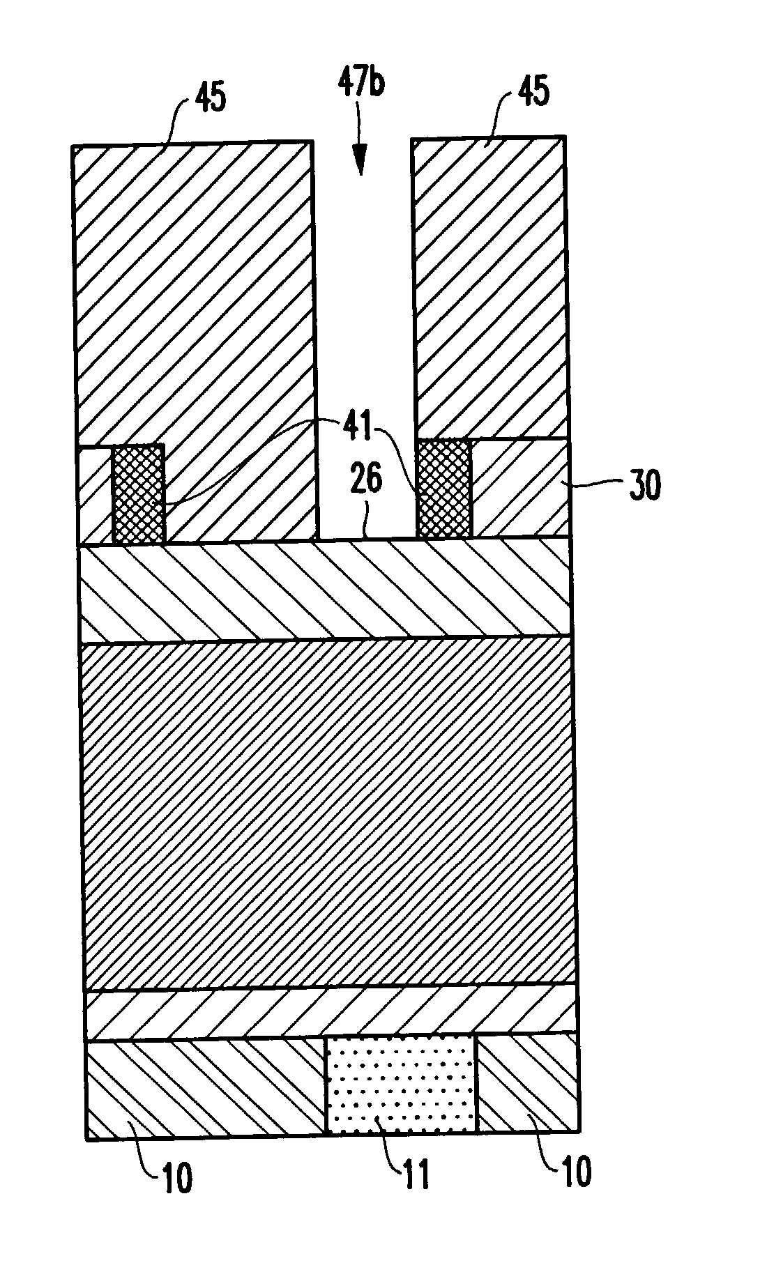
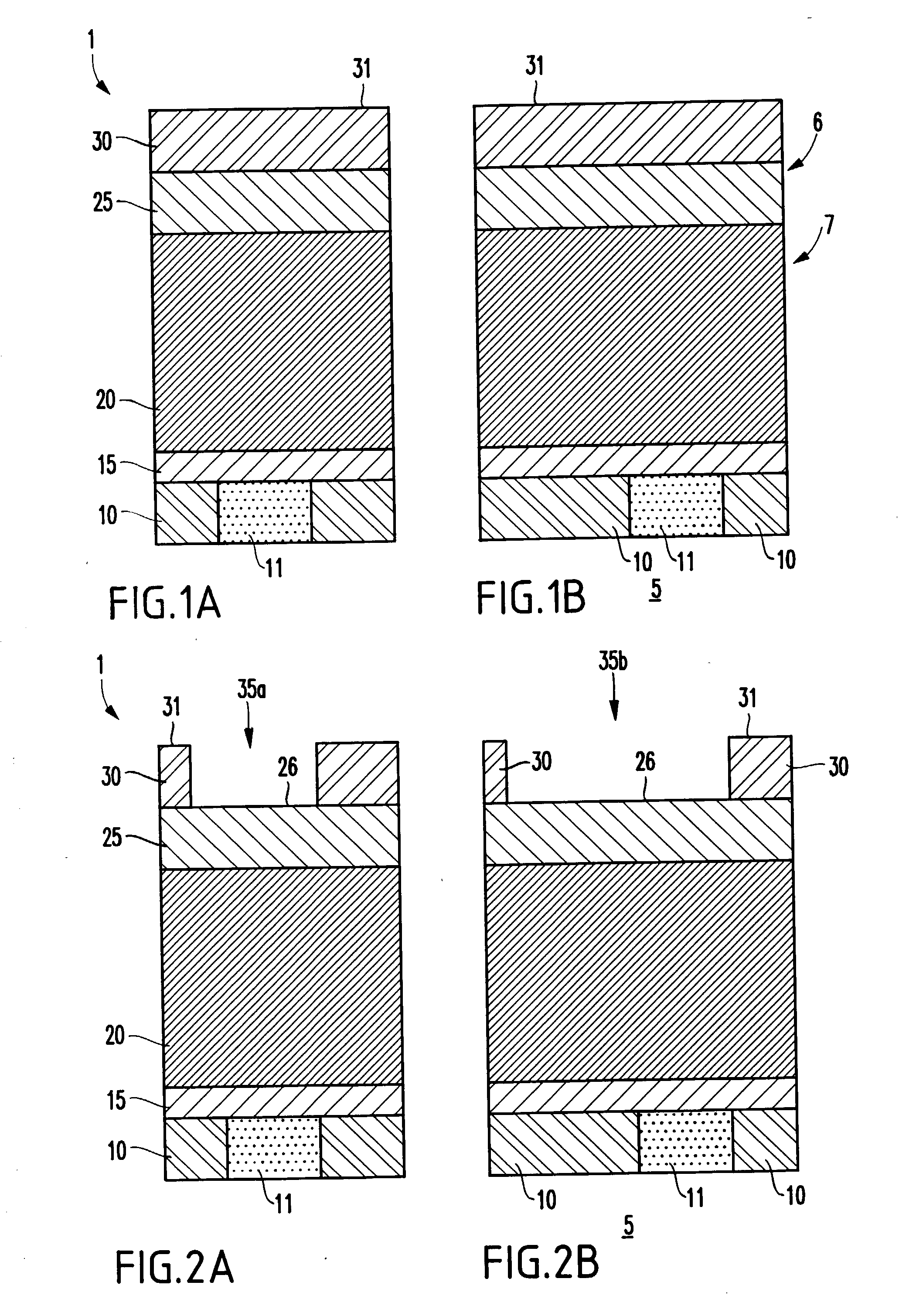
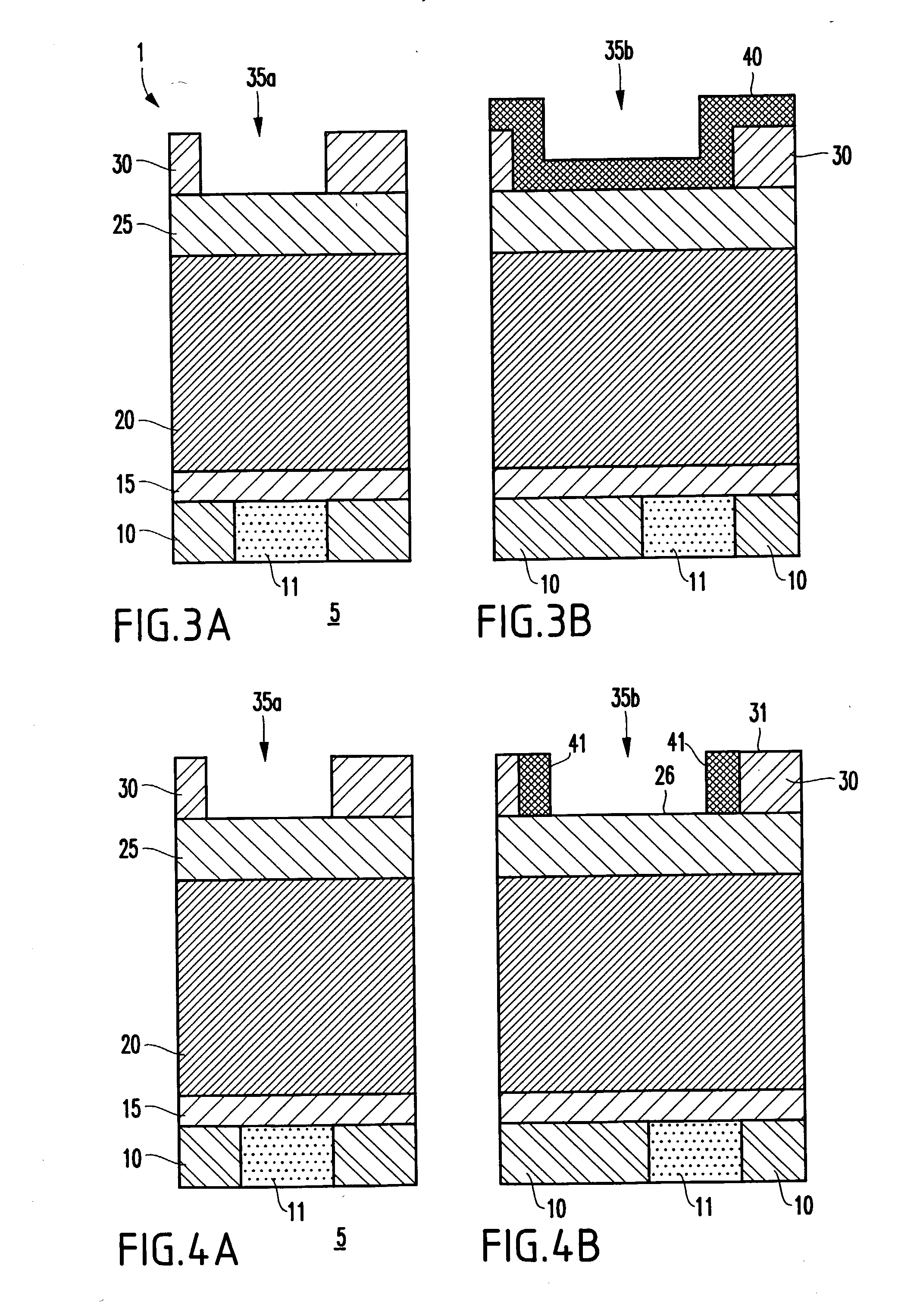
[0049] In a first embodiment shown in FIGS. 1A-12B metal spacers are applied along the sidewalls of a low-k dielectric layer, such as SiLK.RTM.. In this trough first, via second dual damascene integration scheme, the troughs are defined into a hardmask, the vias are defined and etched into the SiLK.RTM., and the trough hardmask pattern is used as a mask to etch the troughs into the SiLK.RTM.. The metal spacer, which is preferably tungsten, but may comprise other materials, such as tantalum nitride, adds a systematic trim to the trough opening which increases the lithographic process window.

[0050] FIGS. 1A, 2A, 3A, 4A, 5A, 6A, 7A, 8A, 9A, 10A, 11A, and 12A illustrate processing without the inventive spacers 41, while FIGS. 1B, 2B, 3B, 4B, 5B, 6B, 7B, 8B, 9B, 10B, 11B, and 12B illustrate the advantages produced by the spacers. The following discussion explains both series of "A" and "B" Figures similarly, except where differences exist. FIG. 1 shows a first embodiment of the present i...

second embodiment

[0061] A second embodiment is shown in FIGS. 13 through 26. This embodiment illustrates the structure and method of fabricating dual damascene troughs / vias into an oxide / PAE stack. The advantage of using a dual oxide / PAE stack is that the oxide can provide mechanical support to the wires fabricated in PAE, the oxide acts as an oxygen / water diffusion barrier, and also the oxide is a very efficient thermal conductor. Additionally, the adhesion of the metallized via bottom to the underlying metal is improved by fabricating it in oxide rather than in PAE.

[0062] FIG. 13 shows a partially completed integrated circuit device 101 comprising a plurality of insulator layers 107 stacked on a substrate 105. A metallization layer 110 is deposited over the substrate 105. The metallization layer 110 comprises wiring conductors 111 therein. Above the metallization layer 110 and wiring conductors 111 is a first nitride insulating barrier layer 115. Above the first nitride layer 115 is an insulating ...

third embodiment

[0079] FIG. 33 illustrates a flow diagram of the present invention, which describes depositing a liner 275, 285 into the vias 235b of the dual damascene interconnect device 201. First, the vias / troughs 235b of the integrated circuit device 201 are cleaned 600. The next step involves optionally performing 605 one of a reactive ion etching and an argon sputter cleaning process. Then, a plurality of metal layers 275, 285 are deposited 610 over the vias / troughs 235b. Finally, copper is deposited 615 in the vias / troughs 235b.

[0080] There are several benefits of the present invention. For example, the present invention provides a novel structure and method for forming a sacrificial metal spacer dual damascene structure as well as a single damascene structure. Also, the present invention provides a new and improved technique of dual damascene and single damascene processing which overcomes the limitations of the conventional designs. Additionally, the present invention improves the dual da...


PUM


Abstract

A method and structure for a dual damascene interconnect structure comprises forming wiring lines in a metallization layer over a substrate, shaping a laminated insulator stack above the metallization layer, patterning a hardmask over the laminated insulator stack, forming troughs in the hardmask, creating sacrificial tungsten sidewall spacers in the troughs, patterning the laminated insulator stack, removing the sacrificial sidewall spacers, forming vias in the patterned laminated insulator stack, and depositing a metal liner and conductive material into the vias and troughs, wherein the laminated insulator stack comprises a dielectric layer further comprising oxide and polyarylene. The step of depositing prevents the laminated insulator stack from sputtering into the vias. Moreover, the step of depositing comprises cleaning the vias and troughs, optionally performing a reactive ion etching or argon sputter cleaning, depositing a plurality of metal layers over the vias and troughs, and depositing copper in the vias and troughs.

Description

[0001] 1. Field of the Invention[0002] The present invention generally relates to integrated circuit design, and more particularly to damascene fabrication using sacrificial metal spacers to aid in the fabrication process.[0003] 2. Description of the Related Art[0004] Dual damascene processing in soft, non-silicon containing intermetal dielectrics, such as SiLK.RTM., available from Dow Chemical Company, NY, USA, or FLARE.RTM., available from Honeywell, NJ, USA (both materials are polyarylenes (PAE)) is extremely difficult at sub 0.25 micron dimensions because of etch bias, undercut corner erosion, etc., and other problems frequent during RIE processing. Additionally, the traditional argon sputter cleans resputtered PAE into the via bottom and onto the underlying metal (i.e. copper or tungsten) surface, resulting in degraded contact interface properties. Although only argon sputtering is given as an example, all methods of directional sputter cleaning, including reactive ion etching ...

Claims


Application Information

Patent Timeline
Patent Type & Authority Applications(United States)
IPC IPC(8): H01L21/768
CPCH01L21/76811H01L21/76844H01L21/76813
Inventor COONEY, EDWARD C. IIIGEFFKEN, ROBERT M.STAMPER, ANTHONY K.
Owner GLOBALFOUNDRIES INC
Why Eureka
Try Eureka