Semiconductor memory device and control method and manufacturing method thereof

a memory device and semiconductor technology, applied in the direction of digital storage, transistors, instruments, etc., can solve the problems of difficult manufacturing of structures in view of process technology, difficult application of salicide processes, and difficult application of silicidation/salicidation processes, etc., to reduce the voltage necessary for program operation, facilitate salicidation, and reduce memory cell size

Inactive Publication Date: 2004-04-15
RENESAS ELECTRONICS CORP
View PDF3 Cites 17 Cited by
  • Summary
  • Abstract
  • Description
  • Claims
  • Application Information

AI Technical Summary

Benefits of technology

[0031] Accordingly, it is an object of the present invention to provide a semiconductor memory device and a manufacturing method thereof which can reduce memory cell size, can facilitate salicidation, and can reduce a voltage necessary for a program operation to a low level.
[0038] In the present invention, when programming is performed, a predetermined positive voltage is applied to the word line connected to the gate electrode of a memory cell to be programmed, a positive program voltage is applied to the second program and erase bit line connected to the memory cell to be programmed, one of the first and third read bit lines connected to the memory cell to be programmed is set to the ground potential, and other bit line is set to a positive program inhibiting voltage. In the present invention, when programming is performed, preferably, the positive program voltage is applied from both sides of the second program and erase bit line, thereby increasing capability of supplying program currents. In other words, a program voltage supplied to the second bit line from one end can be reduced to a low level.

Problems solved by technology

This structure is difficult to be manufactured in view of process technology.
Thus, application of a silicidation / salicidation process, which is commonly employed in a manufacturing process of a logic device is 25 difficult.
However, the configuration shown in FIG. 20, is such a structure to which the application of a salicide process employing commonly used a refractory metal (which has a high melting point) such as W, Mo, Ta, Ti, or the like or a semi-precious metal such as Co is extremely difficult.
An operational failure is thereby caused.
In the memory cell array configuration shown in FIG. 20, the silicidation is extremely difficult.

Method used


Image

  • Semiconductor memory device and control method and manufacturing method thereof
  • Semiconductor memory device and control method and manufacturing method thereof
  • Semiconductor memory device and control method and manufacturing method thereof

Examples


Embodiment Construction

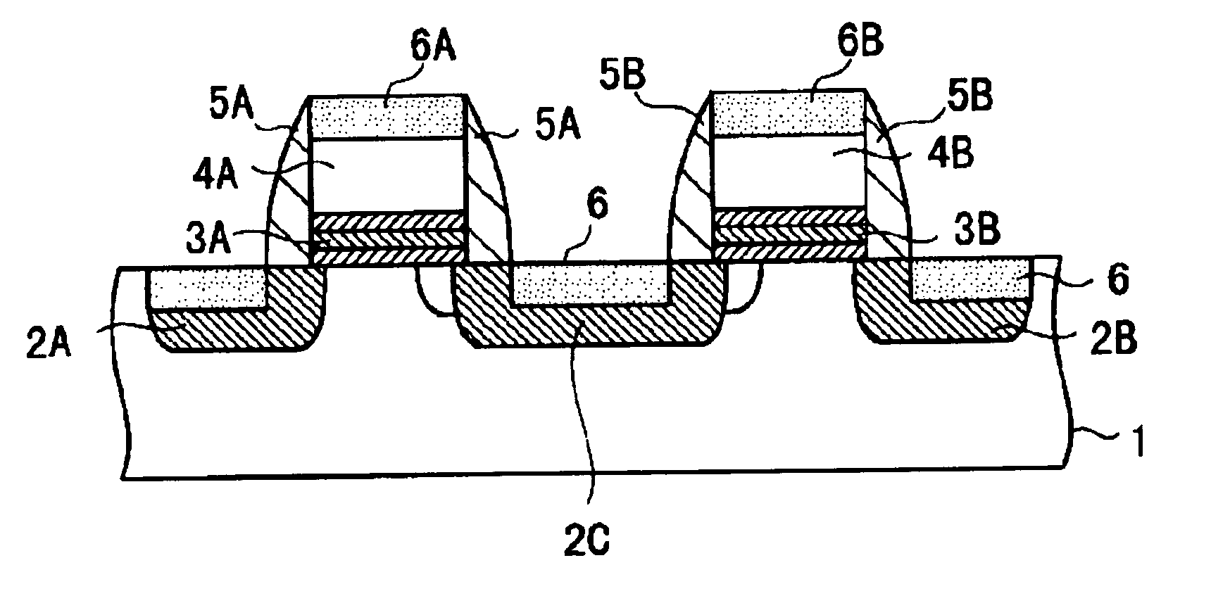
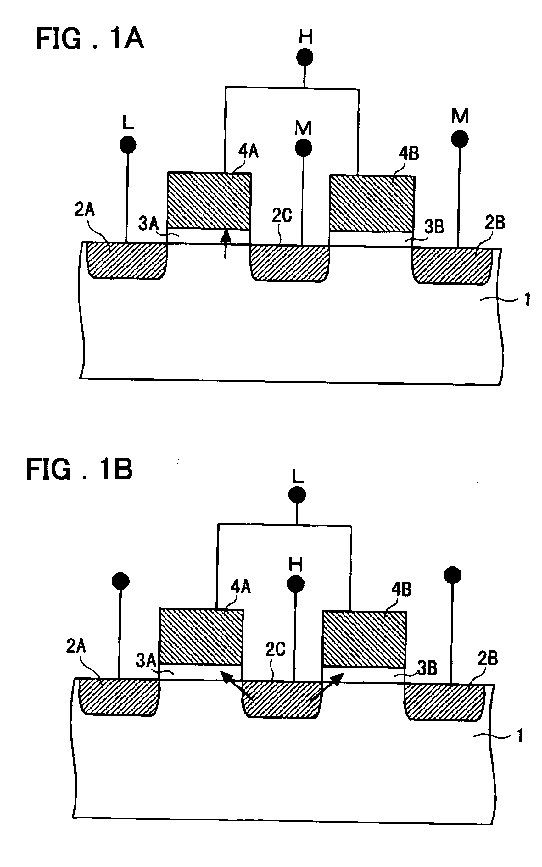
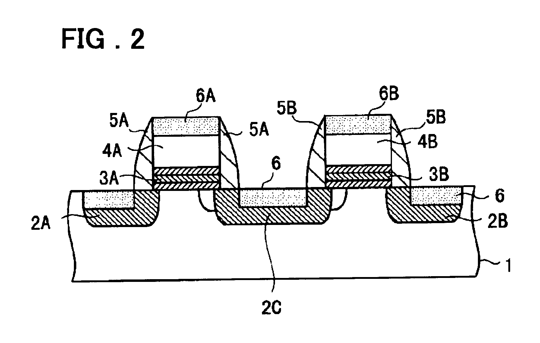
[0077] The preferred embodiment modes of the present invention will be described. In a semiconductor memory device according to an embodiment of the present invention, a cell array has a layout configuration in which each four memory cells shares one contact region and is arranged in an X pattern with the contact region being a center thereof. Referring to FIG. 1, two mutually adjacent memory cells connected to a common word line include first, second and third diffusion regions (2A, 2C, and 2B) provided in a substrate surface and separated to one another, a first insulating film (3A) provided on the substrate to cover a region between the first and second diffusion regions (2A and 2C), a first gate electrode (4A) provided on the first insulating film (3A), a second insulating film (3B) provided on the substrate between the second and third diffusion regions (2B and 2C), and a second gate electrode (4B) provided on the second insulating film (3B).

[0078] A memory cell including the f...


PUM


Abstract

A semiconductor memory device includes a first insulating film provided on a semiconductor substrate between first and second diffusion regions, a first gate electrode provided on the first insulating film, a second insulating film provided on the semiconductor substrate between the second diffusion region and a third diffusion region, and a second gate electrode provided on the second insulating film are included, wherein the first and second diffusion regions, first insulating film, and first gate electrode constitute a first memory cell, while the second and third diffusion regions, second insulating film, and second gate electrode constitute a second memory cell. The first and second gate electrodes are connected in common to form a word line electrode. The first and third diffusion regions are connected to first and second read bit lines disposed on a layer overlying the semiconductor substrate. The second diffusion region is connected to a program and erase bit line disposed on a layer overlying the semiconductor substrate. Programming is performed to a selected memory cell transistor by hot electron injection, while erasing from the selected memory cell is performed by the hot hole injection.

Description

[0001] The present invention relates to a non-volatile semiconductor memory device. More specifically, the invention relates to a MONOS-type flash memory.[0002] As a non-volatile semiconductor memory, such as an electrically erasable and programmable read only memory (EEPROM) device, there is disclosed in Japanese Patent Kokai Publication JP-A-5-174583, an X-cell configuration of a split-gate type non-volatile semiconductor memory device that enabled a high integration being substantially the same as with stack-gate type memory cells. In this split-gate type non-volatile semiconductor memory device, each memory cell has an address gate electrode and a memory gate electrode. Referring to FIGS. 16 and 17, the non-volatile semiconductor memory device described in the above-mentioned Japanese Patent Kokai Publication JP-A-5-174583 will be described. Since the device has a layout configuration in which four memory cells 310, 320, 330, and 340 share one contact region 360 and are disposed...

Claims


Application Information

Patent Timeline
Patent Type & Authority Applications(United States)
IPC IPC(8): G11C16/04H01L21/8247H01L21/8246H01L27/115H01L29/788H01L29/792
CPCG11C16/0416H01L27/11568H01L27/115H10B69/00H10B43/30
Inventor NISHIZAKA, TEIICHIROSAKAI, ISAMIYOSHINO, AKIRAKAWAI, SHINICHIISHIGE, KIYOKAZUHAMAJIMA, TOMOHIROTANAKA, MOTOKO
Owner RENESAS ELECTRONICS CORP
Why Eureka
Try Eureka