Low contamination components for semiconductor processing apparatus and methods for making components

Inactive Publication Date: 2005-01-06
LAM RES CORP
View PDF23 Cites 16 Cited by
  • Summary
  • Abstract
  • Description
  • Claims
  • Application Information

AI Technical Summary

Benefits of technology

[0021] The invention also provides semiconductor processing apparatus that in

Problems solved by technology

This ion bombardment, combined with plasma chemistries and/or etch byproducts, can produce significant erosion, corrosion and corrosion-erosion of the plasma-exposed surfaces of the processing chamber.
This attack causes problems including short part lifetimes, increased consumable costs, particulate contamination, on-wafer transition metal contamination and process drift.
However, these parts are continuously attacked by the plasma and, consequently, ultimately erode or accumulate polymer buildup.
Eventually, these

Method used


Image

  • Low contamination components for semiconductor processing apparatus and methods for making components
  • Low contamination components for semiconductor processing apparatus and methods for making components
  • Low contamination components for semiconductor processing apparatus and methods for making components

Examples


Embodiment Construction

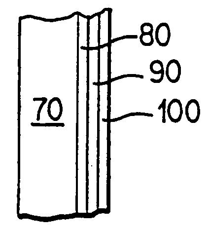
[0030] The invention provides components that have wear resistance with respect to physical and chemical attack by plasmas generated in semiconductor material processing apparatuses. As used herein, the term “wear resistant” includes, but is not limited to, erosion, corrosion and / or corrosion-erosion resistance. The components are composed of wear resistant ceramic materials.

[0031] In some exemplary embodiments, the components include coatings composed of erosion resistant ceramic materials formed on substrates. For example, the components can include substrates and one or more erosion resistant ceramic coatings formed on the substrates. The coatings resist erosion and, being non-metallic materials, are also resistant to corrosion and / or corrosion-erosion.

[0032] In other exemplary embodiments of the invention, the components can consist essentially of wear resistant ceramic materials. For example, the components can be bulk parts of a semiconductor material processing apparatus.

[...


PUM

PropertyMeasurementUnit
Thicknessaaaaaaaaaa
Adhesion strengthaaaaaaaaaa

Abstract

Components of semiconductor processing apparatus are formed at least partially of erosion, corrosion and/or corrosion-erosion resistant ceramic materials. Exemplary ceramic materials can include at least one oxide, nitride, boride, carbide and/or fluoride of hafnium, strontium, lanthanum oxide and/or dysprosium. The ceramic materials can be applied as coatings over substrates to form composite components, or formed into monolithic bodies. The coatings can protect substrates from physical and/or chemical attack. The ceramic materials can be used to form plasma exposed components of semiconductor processing apparatus to provide extended service lives.

Description

BACKGROUND OF THE INVENTION [0001] 1. Field of the Invention [0002] The invention relates to components for semiconductor material processing equipment. The components are formed of materials that can reduce contamination during semiconductor material processing. The invention also relates to methods of making the components. [0003] 2. Description of the Related Art [0004] In the field of semiconductor material processing, vacuum processing chambers are used for etching and chemical vapor deposition (CVD) of materials on substrates. Process gases are flowed into the processing chamber while a radio frequency (RF) field is applied to the process gases to generate a plasma of the process gases. The plasma performs the desired etching or deposition of selected materials on wafers. Examples of parallel plate, transformer coupled plasma (TCP™), which is also called inductively coupled plasma (ICP), and electron-cyclotron resonance (ECR) reactors and components thereof are disclosed in co...

Claims


Application Information

Patent Timeline
IPC IPC(8): C23C4/02C23C4/10C23C14/56C23C16/44C23C28/00C23C30/00H01J37/32H01L21/205H01L21/3065
CPCC23C4/02Y10T428/265C23C14/564C23C16/4404C23C28/00C23C28/34C23C30/00H01J37/32495C23C28/042C23C28/044C23C28/322C23C28/341C23C28/3455C23C28/347C23C28/345Y10T428/263Y10T428/26Y10T428/264C23C4/10C23C14/56C23C16/44H01J37/32
Inventor O'DONNELL, ROBERT J.
Owner LAM RES CORP
Why Eureka
Try Eureka