Semiconductor device

a semiconductor and semiconductor technology, applied in the direction of organic semiconductor devices, solid-state devices, semiconductor devices, etc., can solve the problems of poor directional characteristics, poor color purity, and inability to use light as laser light, and achieve low cost, high performance, and high speed

Inactive Publication Date: 2005-01-13
SEMICON ENERGY LAB CO LTD
View PDF28 Cites 29 Cited by
  • Summary
  • Abstract
  • Description
  • Claims
  • Application Information

AI Technical Summary

Benefits of technology

[0009] In view of the foregoing, it is an object of the present invention is to provide a semiconductor device having an integrated circuit form

Problems solved by technology

However, light emitted from an organic electroluminescent device has generally a comparative wide wavelength band (poor color purity) and poor directional characteristics.
Hence, the

Method used


Image

  • Semiconductor device
  • Semiconductor device
  • Semiconductor device

Examples


example 1

[0122] In Example 1, an example in which CPU core of a CPU (Central Processing Unit) represented by a microprocessor is formed over a plurality of glass substrates to connect the substrates with each other by optical interconnection will be explained.

[0123] A TFT formed over a glass substrate operates at slower than a single crystal transistor. Accordingly, in the case that a CPU is formed over a glass substrate, it is difficult to execute processing at sufficient speed by a single CPU core when the processing is complicated. Consequently, series of processing of a CPU core are divided into some pieces of processing on a subjective basis, and one CPU core formed over a substrate is allocated to each processing. By connecting a plurality of substrates provided with each CPU core by optical interconnection, series of processing can be executed similar to the case of using single CPU core. CPU core formed over each substrate may execute only allocated processing; the processing speed ...

example 2

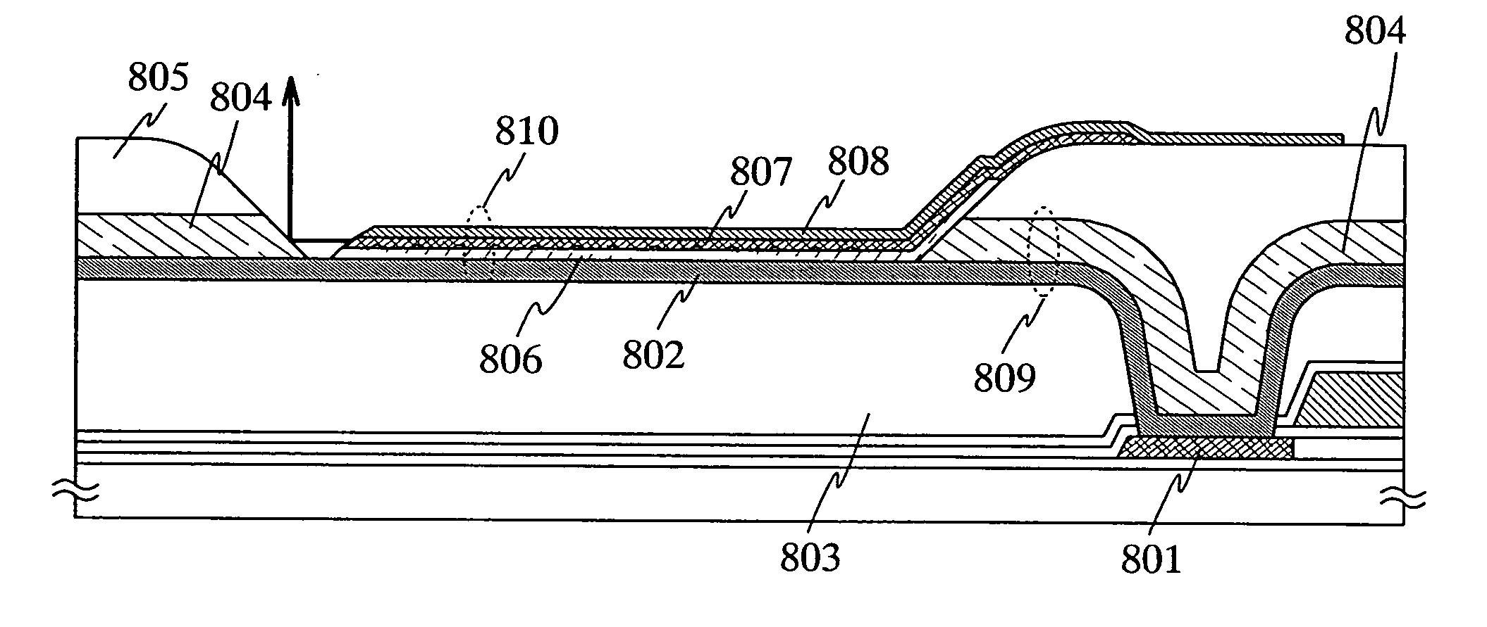
[0136]FIG. 7 shows the device configuration of a sample manufactured according to Example 2. An ITO film is deposited by sputtering to have a thickness of 100 nm as an anode 301 over a support medium over which an electrode, a light-emitting layer, and the like are formed.

[0137]α-NPD is deposited thereover by vacuum vapor-deposition to have a thickness of 135 nm as a hole transporting layer 302. Then, diffraction gratings 307 are formed over the hole transporting layer 302, and then, a light-emitting layer 303 is formed to have a thickness of 30 nm by co-evaporation of 4,4′-bis(N-carbazolyl)-biphenyl (hereinafter, CBP) as a host material and an iridium complex, Ir(tpy)2(acac), which is a triplet light-emitting material. The weight ratio of the CBP and the iridium complex is 10:1. BCP, calcium fluoride (CaF2), and aluminum (Al) are deposited sequentially over these films as an electron transporting layer 304, an electron injecting layer 305, and a cathode 306, respectively. Therefor...

example 3

[0155] An example of a semiconductor display device, which is one of the semiconductor device according to the present invention, will be explained in Embodiment 3.

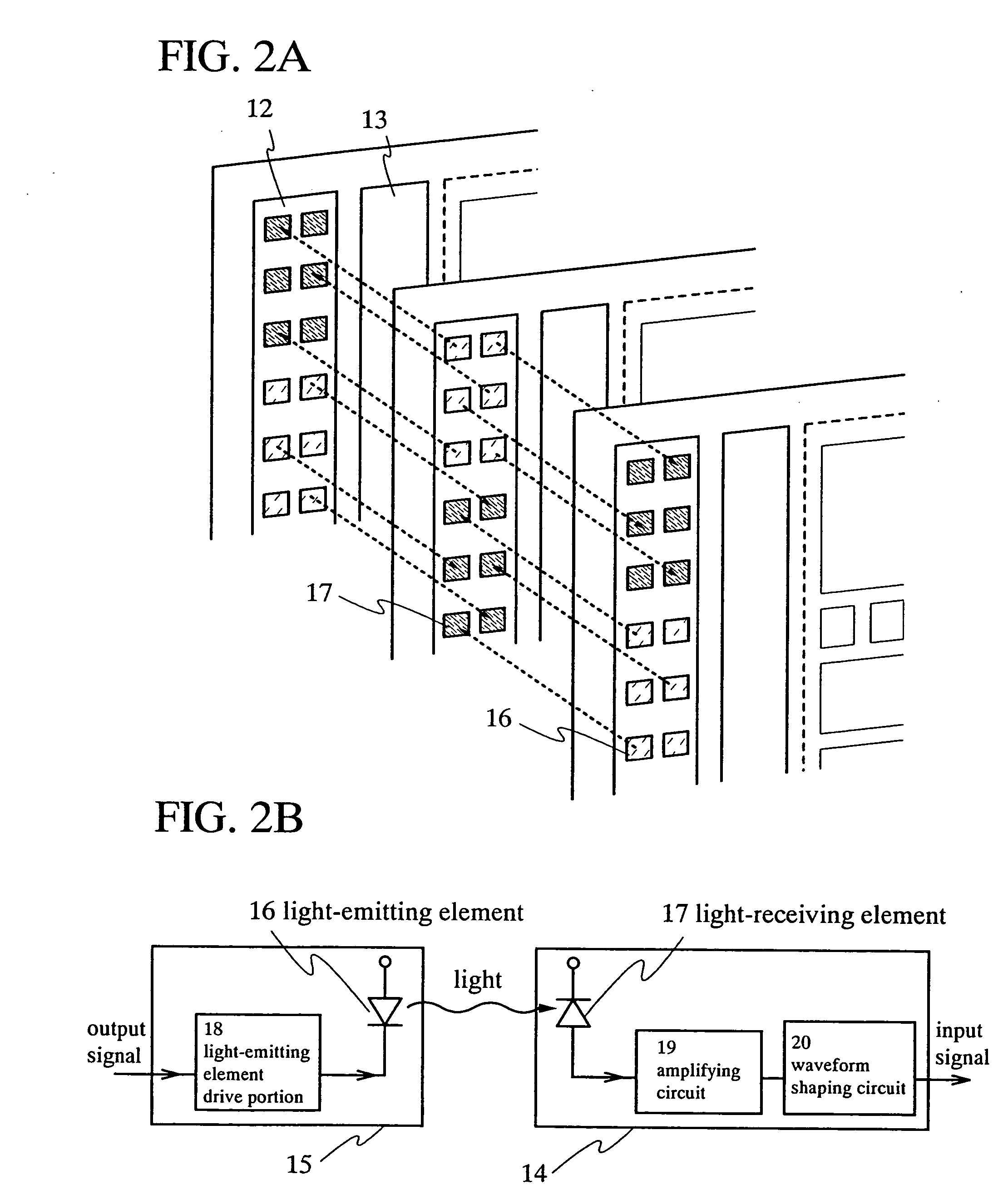
[0156]FIG. 12 is a block diagram for showing the structure of a semiconductor display device according to Example 3. The semiconductor display device shown in FIG. 12 has two glass substrates. An external input terminal 225, a VRAM (Video Random Access Memory) 201, a timing signal generation circuit 202, a video signal processing circuit 203, a light output unit for control signal 204, and a light output unit for video signal 205 are provided to a first substrate 200.

[0157] One or a plurality of light-emitting elements 220 and light-emitting element drive units 221 corresponding respectively to the foregoing light-emitting element are provided to each of the light output unit for control signal 204 and the light output unit for video signal 205. Further, one light-emitting element drive unit 221 may correspond to either...


PUM


Abstract

The present invention provides a semiconductor device having an integrated circuit formed by a low cost glass substrate, which can respond to the increase of an amount of information, and which offers high performance at high speed. A semiconductor device comprises a plurality of glass substrates respectively provided with a circuit including a semiconductor element, in which each of the plurality of glass substrates has both or either of a light-emitting element and/or a light-receiving element; wherein the light-emitting element is formed to have an electroluminescent layer interposed between a pair of electrodes, in which the electroluminescent layer is formed by stacking a plurality of layers capable of emitting light each other so that laser light is oscillated upon applying current to the electroluminescent layer; and a signal is transmitted among circuits formed over the plurality of glass substrates by generating a light signal using the laser light oscillated from the light-emitting element and converting the light signal into an electrical signal in the light-receiving element.

Description

BACKGROUND OF THE INVENTION [0001] 1. Field of the Invention [0002] This invention relates to a semiconductor device composed of a semiconductor film having a crystalline structure formed over a glass substrate, in which a signal is transmitted by light interconnection. [0003] 2. Related Art [0004] A thin film transistor (TFT) formed over an insulating substrate or an insulating film has advantageous features that it can be manufactured easier than an MOS transistor, which is formed over a silicon wafer, and it can be manufactured at low cost by using a large substrate. Especially, since a TFT in which an active layer is formed by a polysilicon film (polycrystalline TFT) has larger mobility than that of a TFT including amorphous silicon, it is expected that the polycrystalline TFT is not only applied to a display device or photoelectric conversion but also widely applied to a functional device including a field of an integrated circuit. [0005] However, an electrical characteristic o...

Claims


Application Information

Patent Timeline
IPC IPC(8): H01L27/12H01L27/32H01L31/16H01L51/50H01L51/52H01S5/30
CPCH01L27/12H01L27/3227H01L27/3248H01L31/16H01L51/5016H01S5/30H01L51/5221H01L51/5265H01L51/5271H01L2251/5315H01L51/5218H10K59/60H10K59/123H10K50/11H10K2101/10H10K50/818H10K50/828H10K50/852H10K50/856H10K2102/3026
Inventor YAMAZAKI, SHUNPEINOMURA, RYOJIABE, HIROKOYUKAWA, MIKIOARAI, YASUYUKI
Owner SEMICON ENERGY LAB CO LTD
Why Eureka
Try Eureka