I have realized that, with the very small spot size used with small
metal links, the heat may be considered to spread in essentially an exponential gradient by conduction from the portion of the beam striking the target. By employing a peak beam power so high that sufficient energy for
evaporation of the link is delivered in a pulse of 8 nanoseconds, and preferably substantially less, the conductive component of
heat transfer can be substantially confined to a
metal link and the underlying
oxide layer, despite its being very thin, such that the temperature rise in the silicon attributable to conduction and the temperature rise attributable to absorption of the beam in silicon, can cumulatively be kept below the temperature threshold at which unacceptable silicon damage occurs.
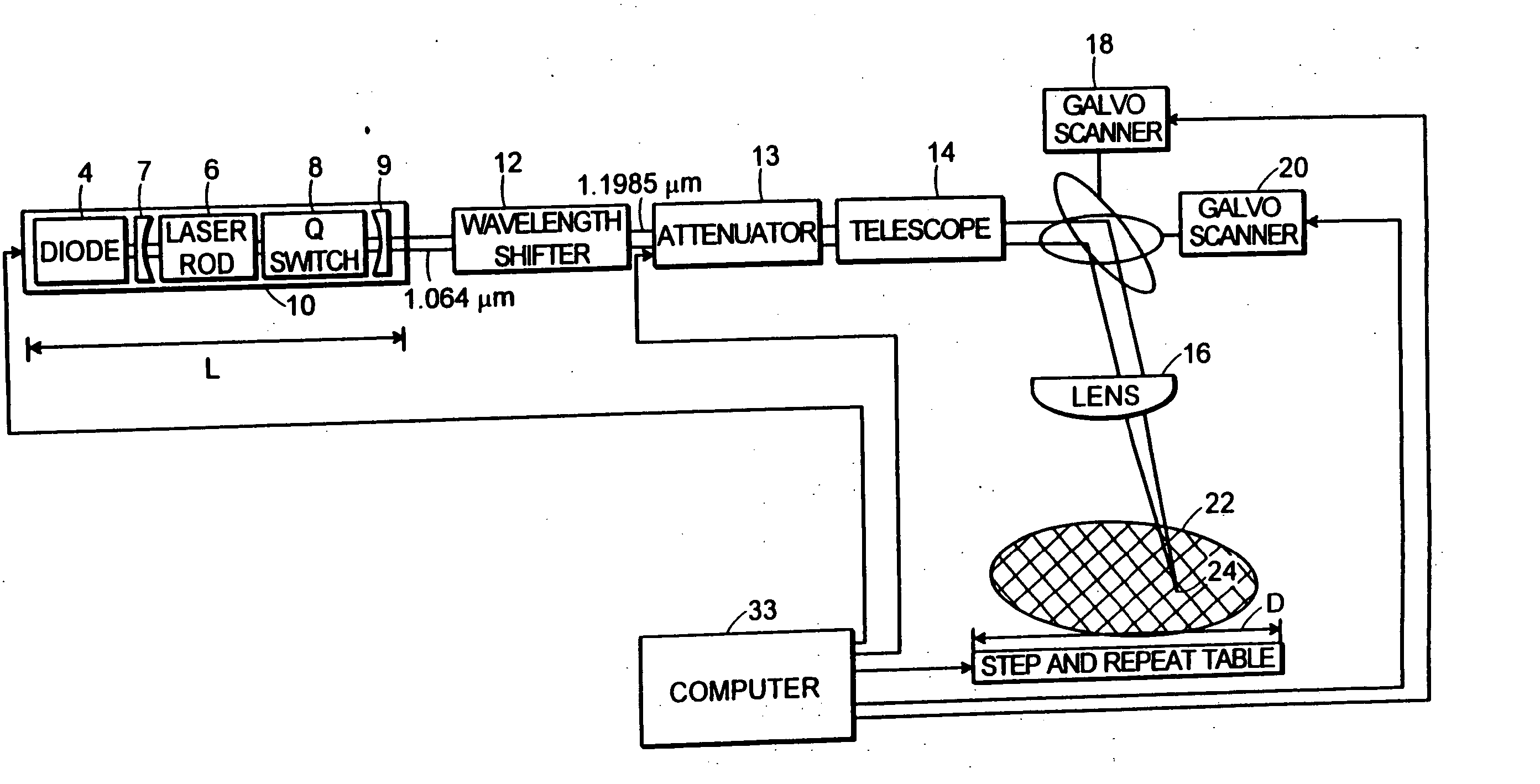
I have further realized that, to achieve the results with current practical technology, a laser having a wavelength that is not beyond the absorption edge of silicon, capable of high
gain at high repetition rate conditions, should be employed to produce an original output beam and a shifting system should be interposed to shift the wavelength of the beam beyond the absorption edge of silicon. Specifically, I have realized that a laser with a high-
gain wavelength, e.g. at 1.047 or 1.064 microns, shifted to a longer wavelength beyond the absorption edge, can produce the desired short pulse in which the requisite energy is delivered.
By employing a system in which the
pulse rate is thus at least 5 Khz, and preferably 8 Khz or 10 Khz, at a wavelength beyond the absorption edge of silicon with a pulse width of less than 8 nanoseconds, and preferably less than 5 nanoseconds or 4 nanoseconds, one can obtain clean removal of a link without leaving conductive residue.
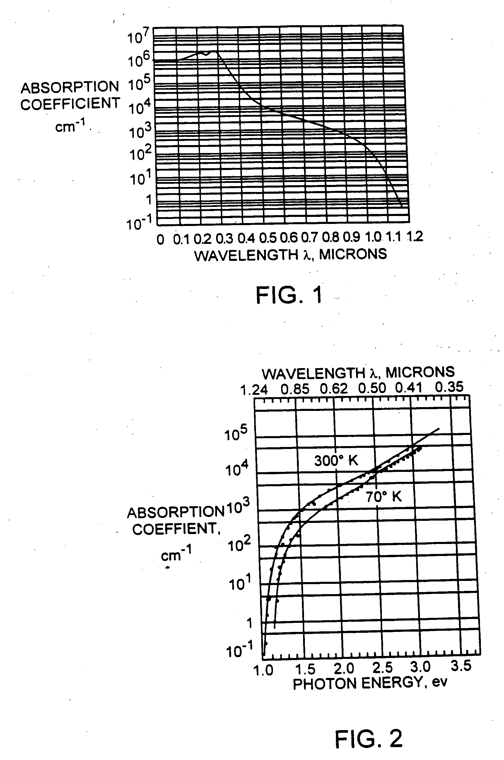
Furthermore, I have realized that by observing an upper limit on the wavelength of less than about 1.2 μm, the overall process
advantage of better focusability gained at such wavelength can outweigh any
advantage that could otherwise be obtained by using longer wavelengths at which the absorption of silicon is more minimized. The sharpness of spot size and good
depth of focus lead to reliable
processing of very large die such as are carried on an 8-inch
wafer, which may have significant variation in flatness over the die surface. In particular, many 8-inch wafers are less than about 300 microns thick and suffer a condition sometimes referred to as the “potato
chip” effect, in which the surface curves or otherwise is not flat. The smaller spot size and better
depth of focus obtainable by maintaining the wavelength less than 1.2 μm can improve the defect rate with such wafers in excess of what might be obtained when longer wavelengths, e.g. 1.32 μm, are employed.
Thus, very clean removal of metal links of current design, e.g. of 1 micron width and ⅓ micron thickness, can be obtained, with high
throughput of memory repair and with relatively few rejects.
According to another aspect of the invention, an optical system is employed to accurately focus a laser spot when operating at a wavelength that is not beyond the absorption edge and the same optical system is used, without modification, at a wavelength beyond the absorption edge, constrained less than 1.2 μm. This provides a versatile new laser system that can be inexpensively retrofitted into existing laser systems. For instance, the initial 1.064 μm laser beam output of the system is useful directly for
processing conventional polysilicide or polysilicon links, and, with the same optical system, using the constrained.
wavelength range beyond the silicon absorption edge, but less than 1.2 μm, fine metal links can be processed. Depending upon the work load of the particular production facility the
optics of the system are optimized at one or the other of the working wavelengths.

