

Manufacturing method for display device
- Summary
- Abstract
- Description
- Claims
- Application Information
AI Technical Summary
Benefits of technology
Problems solved by technology
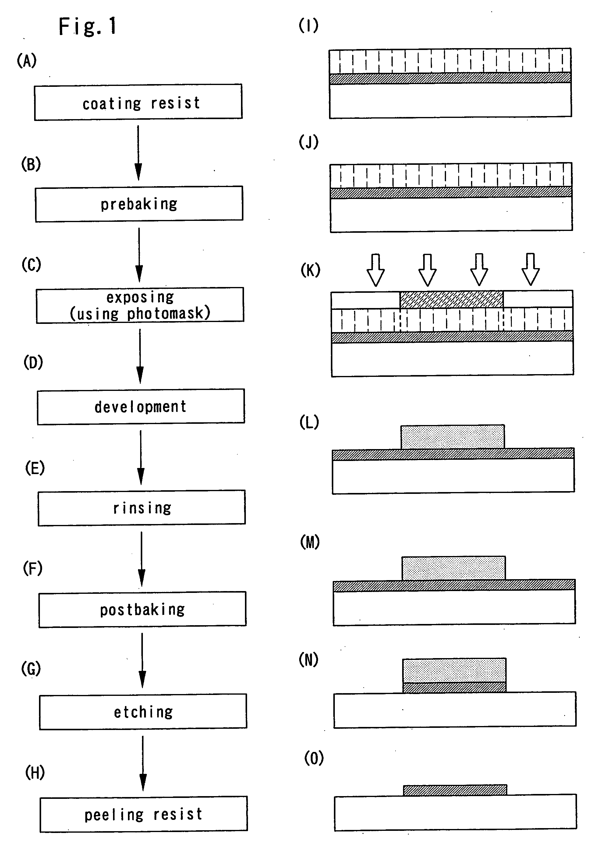
Method used
Image

Examples
embodiment mode 1
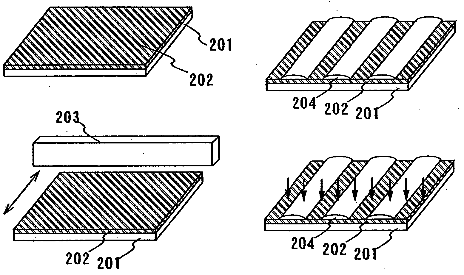
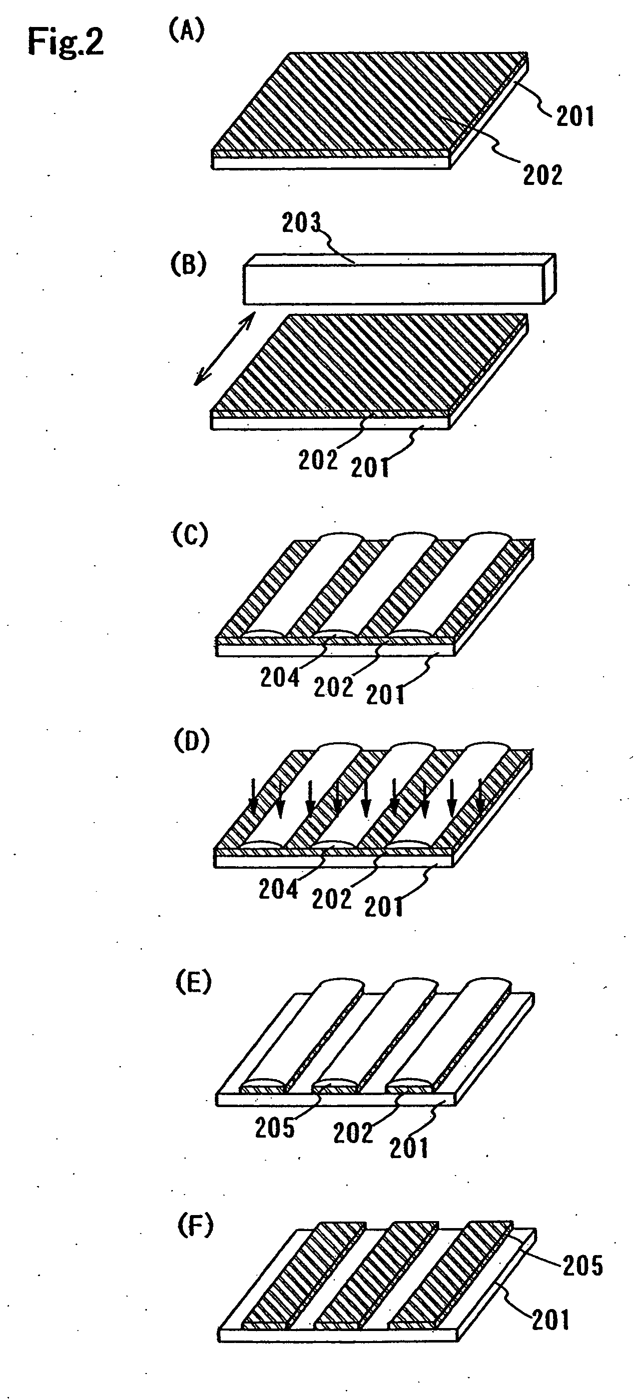
[0035] In an Embodiment mode of the invention, an wiring pattern of a semiconductor device on a glass substrate of a desired size is formed by using liquid drop ejectors and a plasma processing apparatus having a plasma generation means at or near atmospheric pressure. The invention is especially intended for application to a substrate of increasing in size such as of the fifth generation (e.g., 1000×1200 mm or 1100×1250 mm) or of the sixth generation (e.g., 1500×1800 mm). Embodiment mode 1 of the invention is hereinafter described with reference to FIG. 2 that is an accompanying drawing.
[0036] Note that the expression “liquid drop ejectors” simply referred to in Embodiment mode 1 embraces both a liquid drop ejector fitted with a head having dotlike liquid drop ejection holes and a liquid drop ejector fitted with a head having liquid drop ejection holes consisting of linear arrays of dotlike ejection holes.
[0037] First, a film 202 is formed over a substrate 201 to be processed, us...
embodiment mode 3
[0072] A linear liquid drop ejector that can be used in Embodiment Mode 1 is described with reference to the accompanying drawings. The present apparatus has a liquid drop ejection head in which dotlike liquid drop ejection holes are arranged linearly. FIG. 6(A) is a schematic perspective view showing one example of configuration of the linear liquid drop ejector. Also, FIG. 6(B) is a view showing a head in which nozzles used in this linear liquid drop ejector are arranged.
[0073] The linear liquid drop ejector shown in FIG. 6(A) has the head 606 in the apparatus. A desired liquid drop pattern is obtained on a substrate 602 by ejecting liquid drops thereby. In the present linear liquid drop ejector, a glass substrate of desired size can be used as the substrate 602. In addition, a resin substrate typified by a plastic substrate or a semiconductor wafer or the like typified by silicon may also be used as the substrate 602.
[0074] In FIG. 6(A), the substrate 602 is conveyed into the c...
embodiment mode 2
[0104] Embodiment Mode 2 of the invention fabricates a film pattern on a substrate, especially an interconnected pattern for TFTs. In the present Embodiment Mode, interconnections are selectively formed over the substrate without using photoresist.
[0105] A conductive film 902 is selectively formed by the plasm processing apparatus having the plasma generation means at or near atmospheric pressure used in Embodiment Mode 1 (FIG. 9(B)). The selective etching of the conductive film is done by producing a plasma only on portions of the conductive film where a film is to be formed while making a relative motion between the substrate 901 and plasma generation means 903 in the direction of the arrow (in the left direction in the figure) in FIG. 9(C). An interconnected pattern 904 is formed from the conductive film in this way (FIG. 9(D)).
[0106] In Embodiment Mode 4 of the invention, the step of forming the resist pattern shown in Embodiment Mode 1 is omitted. The process sequence can be ...
PUM
 Abstract
Description
Claims
Application Information