Semiconductor device and method for manufacturing semiconductor device

a semiconductor and semiconductor technology, applied in the direction of semiconductor devices, electrical devices, transistors, etc., can solve the problems of increasing power consumption, difficult mass production, and difficulty in controlling the thickness of high-k films formed

Active Publication Date: 2005-01-20
RENESAS ELECTRONICS CORP
View PDF6 Cites 46 Cited by
  • Summary
  • Abstract
  • Description
  • Claims
  • Application Information

AI Technical Summary

Benefits of technology

[0018] Therefore, the present invention proposes the solution of the above-described problems, and it is the object of the present invention to provide a semiconductor device wherein gate insulating films highly controlled their thickness are formed when a plurality of transistors are formed on a chip, even if the difference between the thickness of the gate insulating films is small, and to provide a method for manufacturing such a semiconductor device.

Problems solved by technology

However, in the case when a silicon oxide film is used as a gate insulating film, if the thickness thereof is 2 nm or less, leak current increases resulting in the increase of power consumption.
Since such a thin silicon oxide film is formed of several atomic layers, it is difficult to form evenly, and since a strict manufacturing control is required to improve the uniformity of film thickness, mass production becomes difficult.
However, it is difficult to control the thickness of the high-k films formed using a CVD (chemical vapor deposition) method so as to have a thickness difference of about 0.2 to 0.4 nm.
However, as described above, it is difficult to control the thickness of a silicon oxide film.
Furthermore, the formation of three gate insulating films is required when three kinds of MISFETs, i.e., MISFET for LOP, MISFET for LSTP, and MISFET for high withstand voltage for peripheral circuits; however, in this case, since the formation and removal of the dummy gate must be repeatedly performed, the number of steps increases resulting in lowered productivity.
Furthermore, since the high-k film initially formed is undergone, in addition to the heat treatment of the PDA (post deposition annealing) step for itself, heat of the PDA step for the high-k film subsequently formed, it becomes difficult to control the film thickness and to secure reliability.
In this case, however, it is also difficult to form a silicon oxide film of a thickness equivalent to the thickness difference between the insulating films of 0.2 to 0.4 nm.

Method used


Image

  • Semiconductor device and method for manufacturing semiconductor device
  • Semiconductor device and method for manufacturing semiconductor device
  • Semiconductor device and method for manufacturing semiconductor device

Examples


first embodiment

[0029] First Embodiment

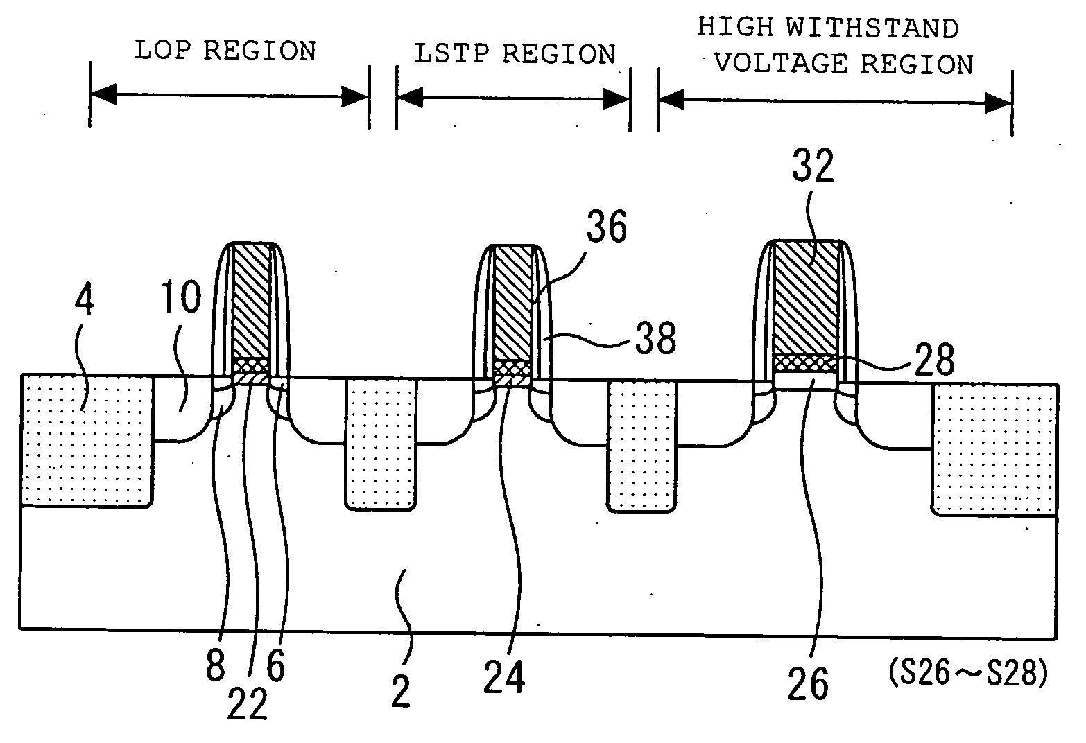
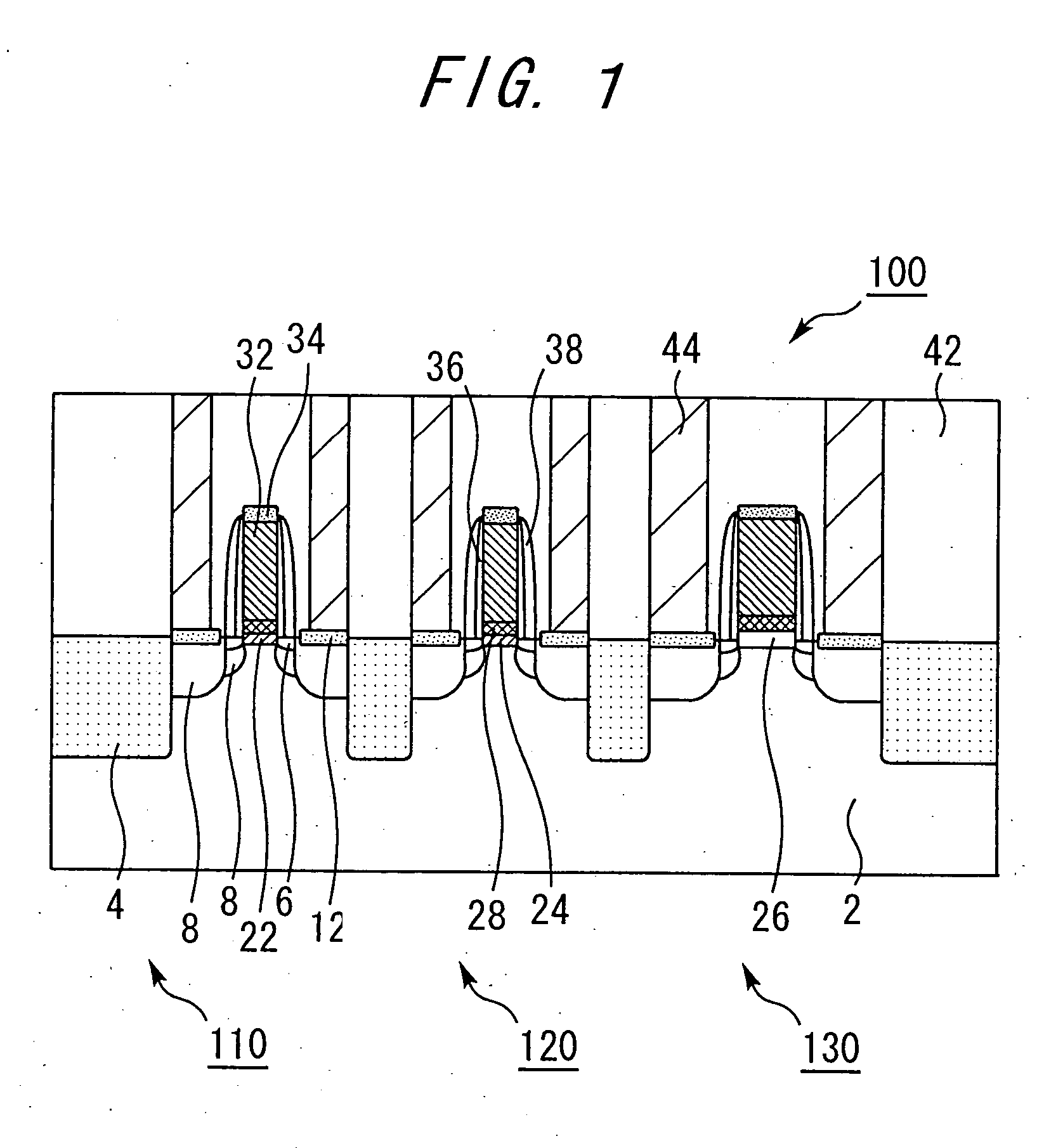
[0030]FIG. 1 is a schematic sectional view for illustrating an SoC (system on chip) 100 according to the first embodiments of the present invention.

[0031] As FIG. 1 shows, the SoC 100 is composed of a MISFET (metal insulator semiconductor field effect transistor) 110 for LOP (low operating power) (hereafter referred to as MISFET for LOP 110); an MISFET 120 for LSTP (low stand-by power) (hereafter referred to as MISFET for LSTP 120); and an MISFET 130 for high withstand voltage (hereafter referred to as MISFET for high withstand voltage 130).

[0032] The MISFETs for LOP 110, for LSTP 120, and for high withstand voltage 130 are formed in regions of an Si substrate 2 isolated by STI (shallow trench isolation) 4., respectively.

[0033] On each region of the Si substrate 2 isolated by STI 4, a source-drain extension 6, which is a diffusion layer having a relatively shallow junction and a low impurity content is formed, and a punch-through stopper 8 is formed underne...

second embodiment

[0075] Second Embodiment

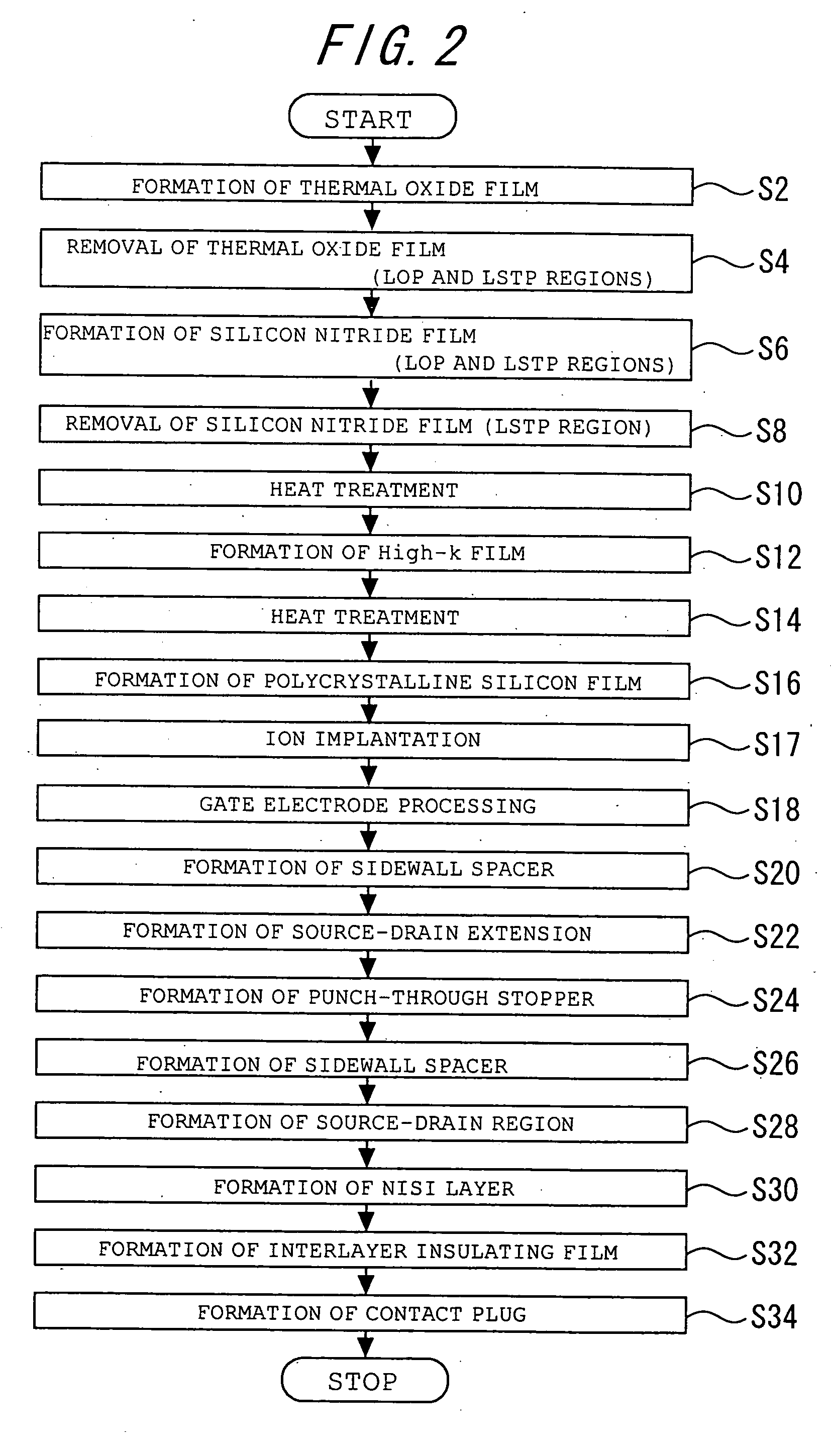
[0076]FIG. 12 is a flow diagram for illustrating the method for manufacturing an SoC according to the second embodiment of the present invention.

[0077] The SoC manufactured in the second embodiment is structurally similar to the SoC 100 described in the first embodiment. However, in the SoC of the second embodiment, the EOT of the silicon oxynitride film 22 of the MISFET for LOP 110 is about 0.7 nm, and the nitrogen content in the silicon oxynitride film is 15 to 25%. The thickness of the silicon oxynitride film 24 of the MISFET for LSTP 120 is about 1.0 nm, and the EOT thereof is also about 1.0 nm. The nitrogen content in the silicon oxynitride film 24 is 1% or less.

[0078] The method for manufacturing an SoC according to the second embodiment is also similar to the manufacturing method described in the first embodiment.

[0079] However, in the second embodiment, the heat treatment in a nitrogen monoxide atmosphere at about 800 to 900° C. for 5 to 60 seconds...


PUM

PropertyMeasurementUnit
thicknessaaaaaaaaaa
thicknessaaaaaaaaaa
thicknessaaaaaaaaaa

Abstract

In a method for forming a semiconductor device, the major surface of a substrate is separated into a first element region for forming a first field-effect transistor and a second element region for forming a second field-effect transistor. A silicon nitride film is formed in each of the first and second element regions. Thereafter, the silicon nitride film formed in the second element region is removed, and the substrate is subjected to heat treatment in an ambient that contains nitrogen oxide. Thereby, the silicon nitride film in the first element region is oxidized to form an oxynitride film, and a silicon oxynitride film is formed in the second element region. Thereafter, a high-dielectric-constant film is formed on the silicon oxynitride films in each of the first and second element regions.

Description

BACKGROUND OF THE INVENTION [0001] 1. Field of the Invention [0002] The present invention relates to a semiconductor device and a method for manufacturing a semiconductor device. More specifically, the present invention relates to a semiconductor device having a plurality of transistors comprising gate insulating films of different film thickness, and a method for manufacturing such a semiconductor device. [0003] 2. Background Art [0004] Concurrent with the advance of the down-sizing technology of semiconductor integrated circuits in recent years, the dimension of an element has been reduced, and a larger number of elements have been able to be mounted in a chip. Therefore, an integrated-circuit device referred to as SoC (system on chip) that can individually realize functions conventionally realized using a plurality of element has been widely used. [0005] In the logic circuit portion of an SoC, it is required to lower the driving voltage for reducing power consumption. At the same...

Claims


Application Information

Patent Timeline
Patent Type & Authority Applications(United States)
IPC IPC(8): H01L21/314H01L21/316H01L21/336H01L21/00H01L21/8234H01L27/088
CPCH01L21/823462H01L21/3144H01L21/02326H01L21/0214H01L21/022H01L21/00H01L21/18H01L21/02337
Inventor TORII, KAZUYOSHIMITSUHASHI, RIICHIROUHORIUCHI, ATSUSHI
Owner RENESAS ELECTRONICS CORP
Why Eureka
Try Eureka