

Method and system for ion beam containment using photoelectrons in an ion beam guide
a technology of ion beam and guide, which is applied in the field of ion beam containment and transport in the ion beam implantation system, can solve the problems of difficult to maintain the convergence of the ion beam, the probability of ionizing collision with the background gas is very low, and the blowup of beams is particularly troublesome, so as to facilitate the attraction of the generated photoelectrons and limit the effect of beam biasing
- Summary
- Abstract
- Description
- Claims
- Application Information
AI Technical Summary
Benefits of technology
Problems solved by technology
Method used
Image

Examples
Embodiment Construction
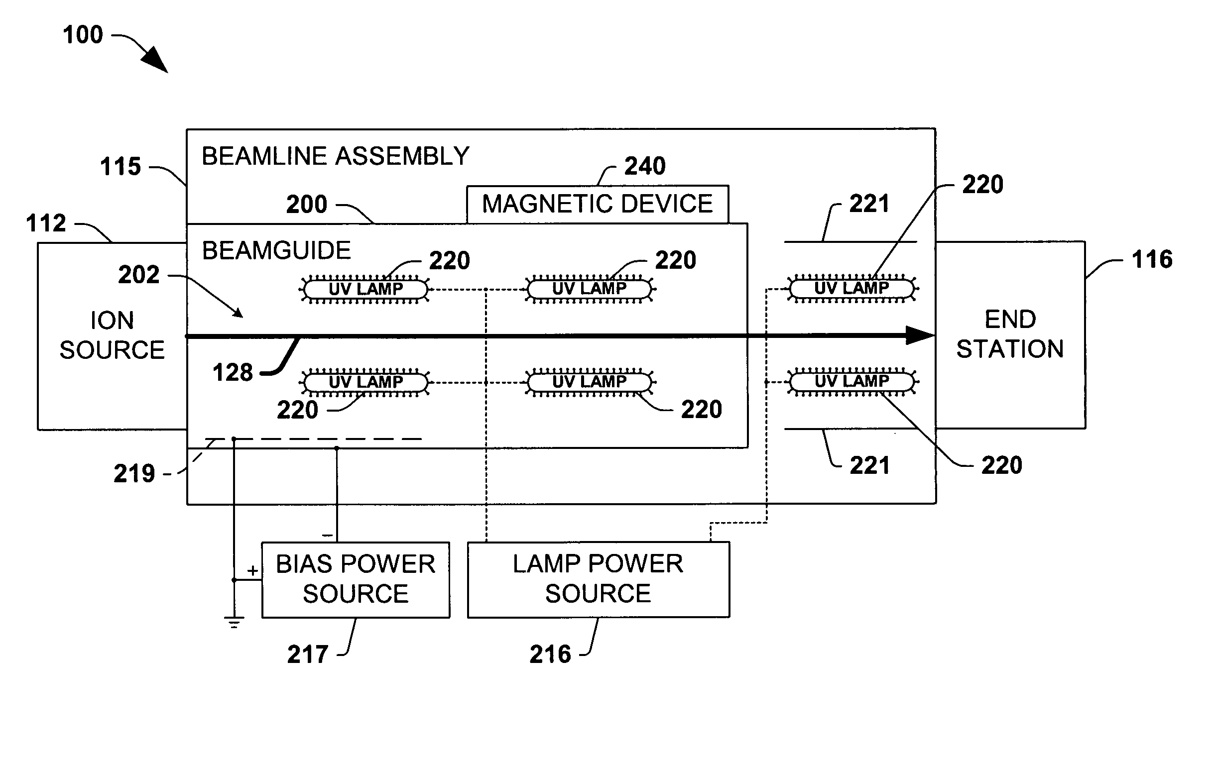
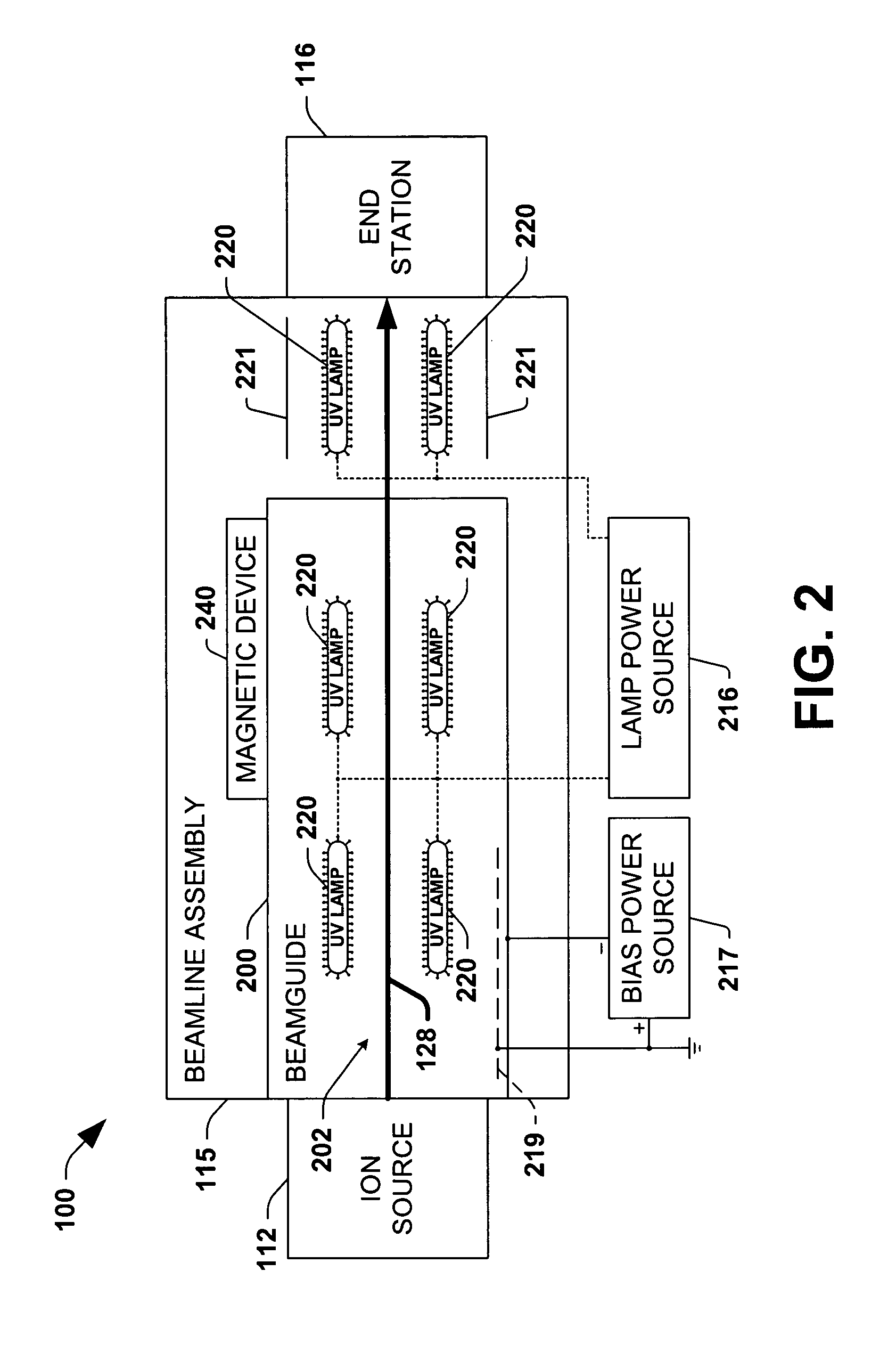
[0027] The present invention will now be described with reference to the drawings wherein like reference numerals are used to refer to like elements throughout. The present invention provides for beam containment or confinement in ion implantation systems, for example, low energy, high current implanters operated at low pressures, without requiring the introduction of plasma into the beamline assembly from an external plasma source, by enhancing the beam plasma using photoelectrons created in the implanter through photoemission. Several examples of low energy implantation systems and beamline assemblies therefor are hereinafter presented in order to illustrate the various aspects of the invention. However, it will be appreciated that the invention may be advantageously employed in ion implanter systems apart from those illustrated and described herein. For example, various exemplary implementations are illustrated and described hereinafter in the context of beam confinement apparatu...
PUM
 Abstract
Description
Claims
Application Information