
Laser processing method and apparatus

Inactive Publication Date: 2005-02-10
KK TOSHIBA
View PDF5 Cites 3 Cited by
  • Summary
  • Abstract
  • Description
  • Claims
  • Application Information

AI Technical Summary

Benefits of technology

[0026] An object of the present invention is to provide a laser processing method and apparatus in which a polycrystalline Si film having a uniform and large particle diameter can be formed with a high throughput.

Problems solved by technology

Since the solid phase growth method is a high-temperature process, it is necessary to use an expensive quartz glass in the glass substrate.
When the movement speed decreases, the enhanced capability of the semiconductor device cannot be expected.
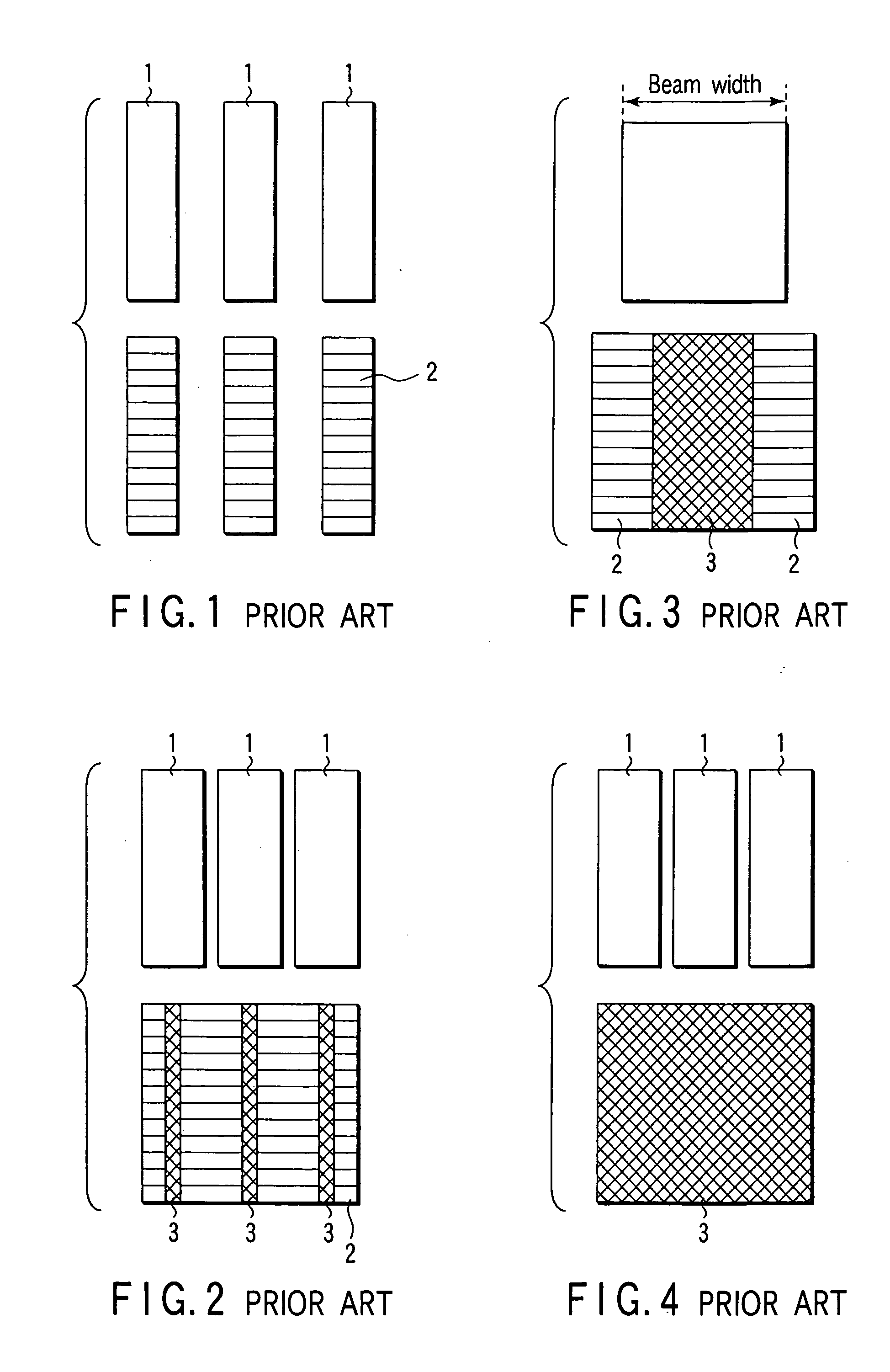
However, in these methods, since the Si thin film is successively irradiated with the laser beam at an interval, the glass substrate has to be moved for each irradiation with the laser beam.
To form the polycrystalline Si film over the large-sized glass substrate, a throughput of several hours is required, and formation cannot be realized.
However, the former method requires a throughput of several hours, is unrealistic, and has a low productivity.
Therefore, the throughput in an actual mass production line is not achieved, and a further high-speed processing is necessary.

Method used


Image

  • Laser processing method and apparatus
  • Laser processing method and apparatus
  • Laser processing method and apparatus

Examples


first embodiment

[0070] the present invention will be described hereinafter with reference to the drawings.

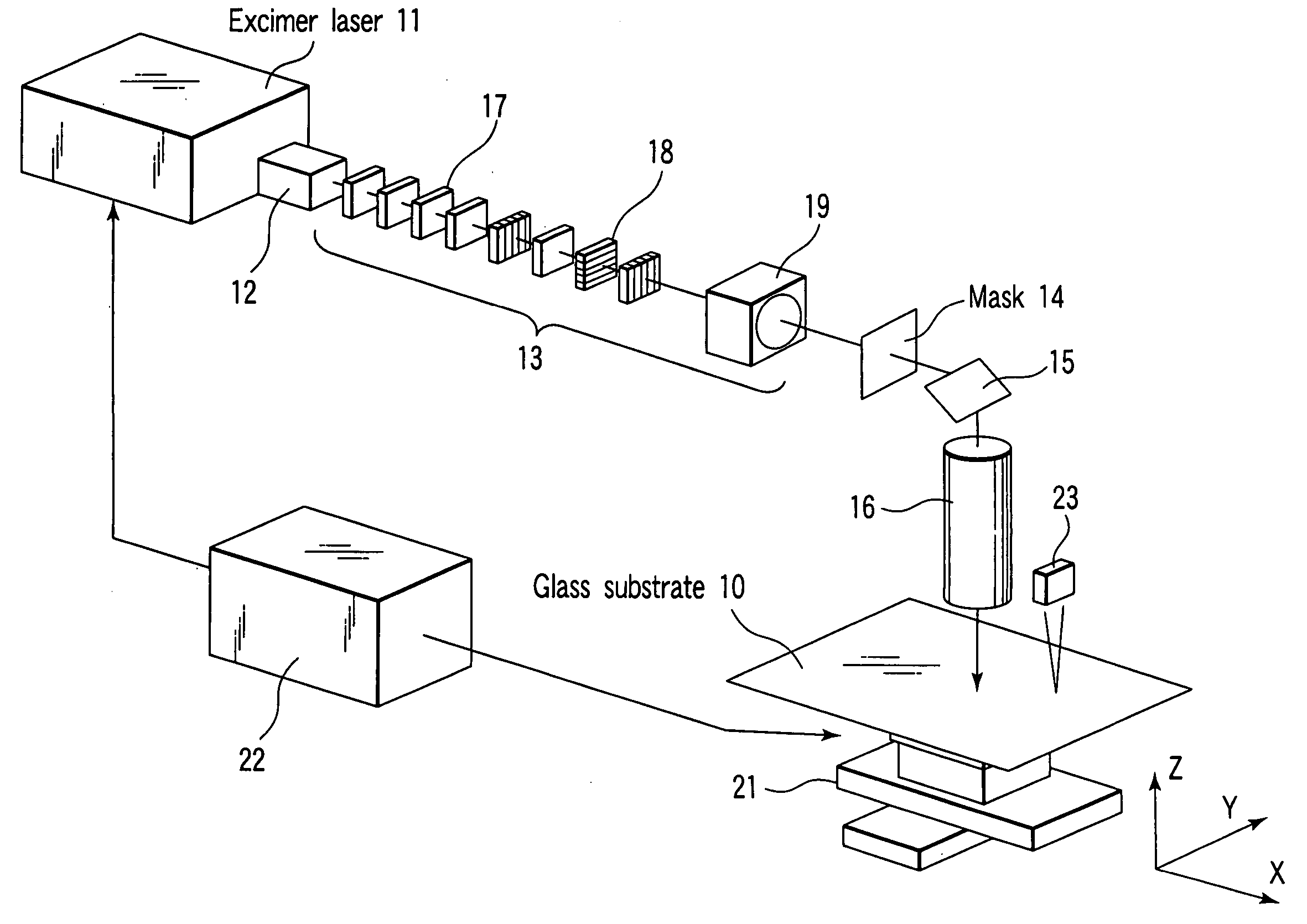
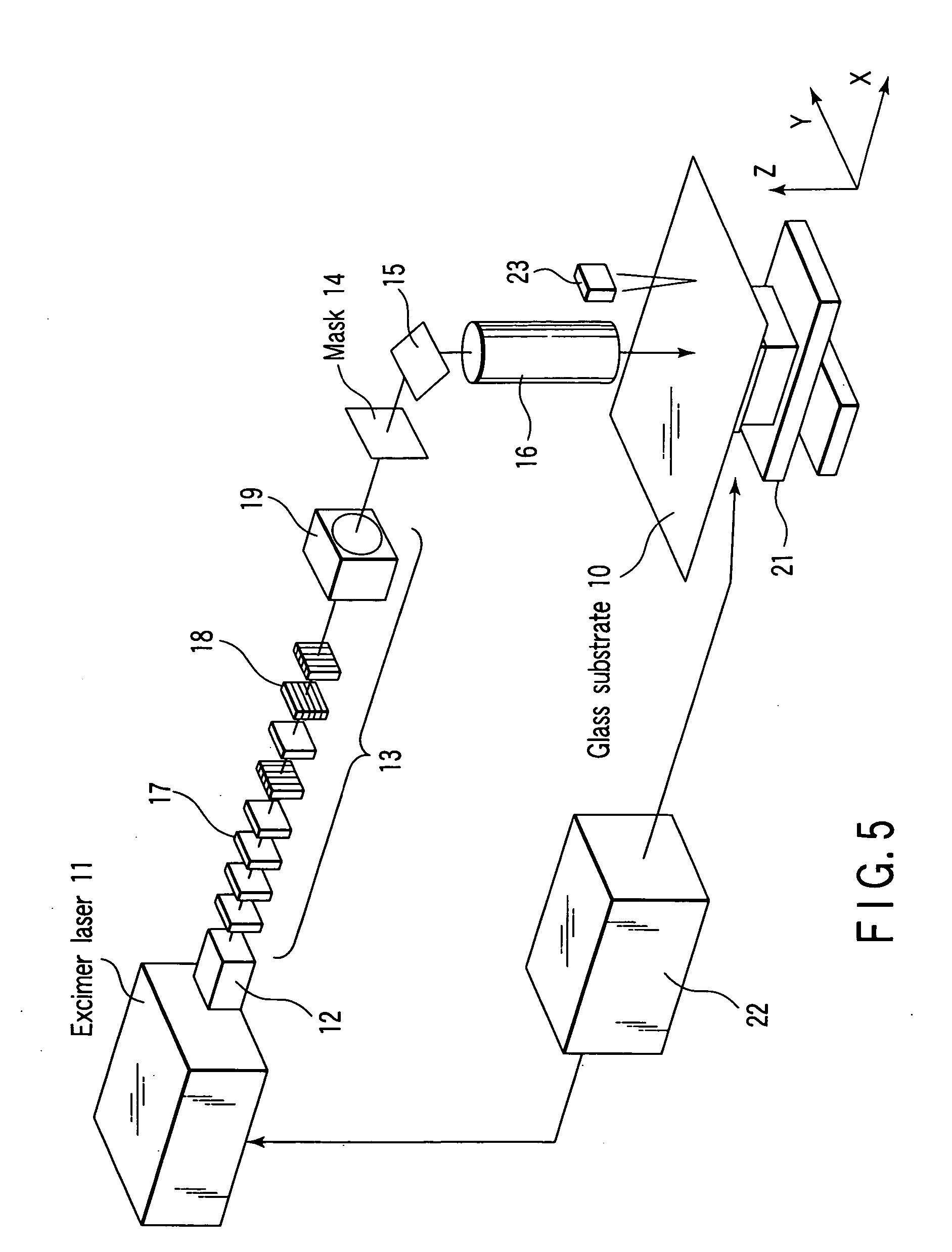
[0071]FIG. 5 is a constitution diagram of a laser processing apparatus. The laser processing apparatus is applied to manufacturing of a p-Si TFT liquid crystal display which has a process of poly-crystallization of an a-Si film formed on a glass substrate 10.

[0072] An excimer laser 11 outputs a pulse laser, for example, at a repeated frequency of 200 to 500 Hz. The excimer laser 11 outputs the pulse laser whose energy density of an irradiated point on the a-Si film is of the order of 200 to 500 J / cm2. The point irradiated with the pulse laser forms a processed point on the a-Si film.

[0073] A variable attenuator 12, lighting optical system 13, mask 14, and mirror 15 are disposed along an optical path of the pulse laser. A projection lens 16 is disposed on a reflected light path of the mirror 15.

[0074] The lighting optical system 13 is constituted of a homogenizer, and a beam shaping optical s...

second embodiment

[0134] the present invention will next be described with reference to the drawings.

[0135] In the laser processing apparatus of the second embodiment, the mask 14 shown in FIG. 5 is modified. Therefore, the laser processing apparatus will be described using the laser processing apparatus shown in FIG. 5.

[0136]FIG. 12 is a constitution diagram of a mask 30 for use in the laser processing apparatus.

[0137] In the mask 30, square patterns 31 as openings are formed in the same direction. The width and pitch of the square pattern 31 are formed in the sizes to form the polycrystalline Si film having the predetermined or larger crystal particle diameter, when the a-Si film is irradiated with the pulse laser and poly-crystallized.

[0138] The width of each square pattern 31 is formed in a slit width length to generate the heat gradient in the laser irradiated region, when the a-Si film is irradiated with the pulse laser. The pitch between the square patterns 31 is formed in the pitch interva...

third embodiment

[0168] the present invention will next be described with reference to the drawings.

[0169] In the laser processing apparatus of the third embodiment, the constitution of the mask 14 shown in FIG. 5 is changed. Therefore, the laser processing apparatus will be described using the laser processing apparatus shown in FIG. 5.

[0170]FIG. 18 is a constitution diagram of a mask 40 for use in the laser processing apparatus.

[0171] In the mask 40, a plurality of dotted openings (hereinafter referred to as a dotted pattern) 41, and a plurality of ring-shaped openings (hereinafter referred to as square ring patterns) 42-1, 42-2 are formed.

[0172] The dotted pattern 41 and square ring patterns 42-1, 42-2 are formed in positions which do not overlap one another in first to third mask regions M21 to M23.

[0173] These dotted pattern 41 and square ring patterns 42-1, 42-2 are formed in the respective widths and pitches such that the heat gradient appears at a time of irradiation of the glass substra...


PUM

PropertyMeasurementUnit
Lengthaaaaaaaaaa
Lengthaaaaaaaaaa
Lengthaaaaaaaaaa

Abstract

There is disclosed a laser processing method including moving a mask and a work with respect to each other while emitting a pulse laser a plurality of times, and moving the mask and the work with respect to each other to form respective laser irradiated regions disposed adjacent to one another by irradiating the work with the pulse laser transmitted through openings formed in positions different from one another on the mask, so that boundaries of the laser irradiated regions disposed adjacent to each other contact at least each other.

Description

CROSS-REFERENCE TO RELATED APPLICATIONS [0001] This application is based upon and claims the benefit of priority from the prior Japanese Patent Application No. 2001-032708, filed Feb. 8, 2001, the entire contents of which are incorporated herein by reference. BACKGROUND OF THE INVENTION [0002] 1. Field of the Invention [0003] The present invention relates to a manufacturing process, for example, of a polysilicon (p-Si) thin film transistor (TFT) liquid crystal display, and to a laser processing method and apparatus in which a workpiece such as an amorphous silicon (a-Si) film is irradiated with a pulse laser beam, and the a-Si film is poly-crystallized. [0004] 2. Description of the Related Art [0005] A manufacturing process of a p-Si TFT liquid crystal display includes a process of poly-crystallization. The process includes: forming an a-Si thin film on a glass substrate of the liquid crystal display; and forming the thin film into a polycrystalline silicon (Si) film. [0006] Example...

Claims


Application Information

Patent Timeline
IPC IPC(8): G02F1/13B23K26/06
CPCB23K26/0656B23K26/066G02F1/13
Inventor ITO, HIROSHI
Owner KK TOSHIBA
Learn More