Semiconductor laser and method for manufacturing the same

Active Publication Date: 2005-02-24
PANNOVA SEMIC
View PDF3 Cites 14 Cited by
  • Summary
  • Abstract
  • Description
  • Claims
  • Application Information

AI Technical Summary

Benefits of technology

[0011] In order to overcome the above-mentioned drawbacks in the conventional examples, it is an object of the present invention to provide a ridge-type stripe structured semiconductor laser having a dielectric film as a current blocking layer, which has a small enough absorption coefficient with respect to an emission wavelength, and has a sufficiently small difference in refracti

Problems solved by technology

With this structure, the MOCVD process is carried out three times in the manufacturing process, thus it is hard to reduce the manufacturing cost.
The increment of the op

Method used


Image

  • Semiconductor laser and method for manufacturing the same
  • Semiconductor laser and method for manufacturing the same
  • Semiconductor laser and method for manufacturing the same

Examples


Example

Embodiment 1

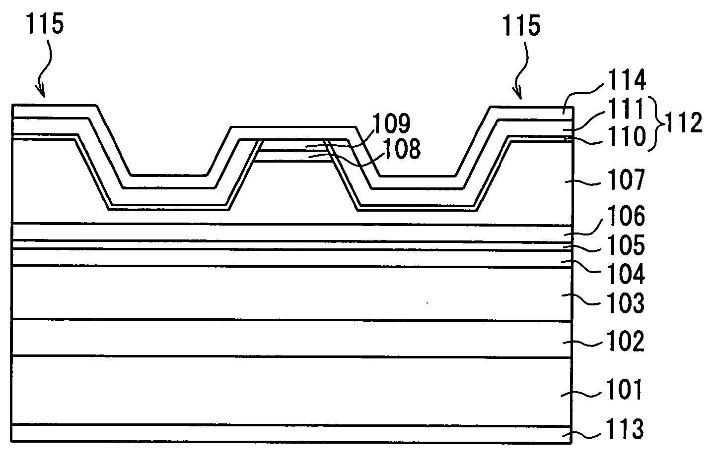
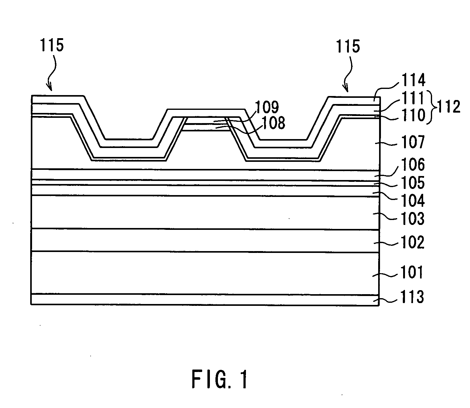
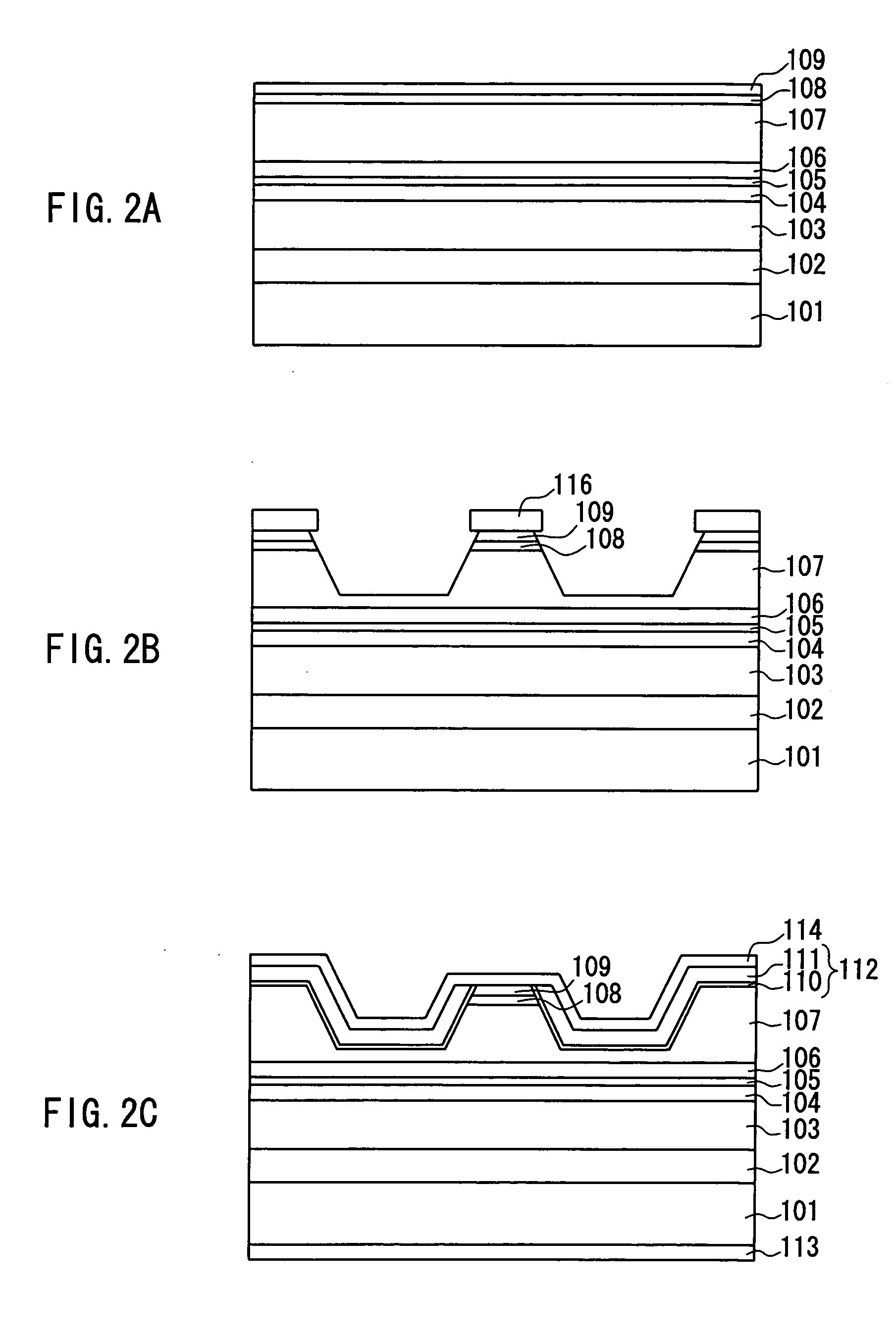
[0043]FIG. 1 is a cross sectional schematic view of an AlGaInP based laser according to Embodiment 1. The semiconductor laser of the present embodiment has a ridge-type stripe structure, in which a n-type GaAs buffer layer 102, a n-type AlGaInP cladding layer 103, an undoped AlGaInP optical guide layer 104, a multiple quantum well active layer 105, an undoped AlGaInP optical guide layer 106, a p-type AlGaInP cladding layer 107, a p-type GaInP hetero buffer layer 108, a p-type GaAs cap layer 109 and a laminated current blocking payer 112 are formed on a n-type GaAs substrate 101, and further, a n-side electrode 113 is formed on the rear face of the n-type substrate 101, and a p-side electrode 114 is formed on the contact layer 109.

[0044] Specific examples of each layer will be described below. The n-type GaAs substrate 101 may be formed of a Si-doped n-type GaAs. The n-type GaAs buffer layer 102 may be formed of a Si-doped n-type GaAs (Si concentration: n=2×1018 cm−3, f...

Example

Embodiment 2

[0066]FIG. 5 is a cross sectional view showing the structure of the semiconductor laser according to Embodiment 2. Since the basic structure thereof is similar to that of the semiconductor laser shown in FIG. 1, the same elements are assigned the same reference numerals and the specific explanations thereof will not be repeated. This semiconductor laser is different from the semiconductor laser according to Embodiment 1 in the point that a current blocking layer 117 has a three layered structure in which the hydrogenated amorphous silicon film 111 is sandwiched between the silicon nitride films 110.

[0067] When hydrogen included in the hydrogenated amorphous silicon film thermally diffuses toward the outside, the diffusion toward the interface with the ridge portion can be prevented by the silicon nitride film, which was described in Embodiment 1. In such a case, hydrogen also diffuses in the reverse direction, that is, toward the interface with the p-side electrode 114...


PUM

PropertyMeasurementUnit
Thicknessaaaaaaaaaa
Thicknessaaaaaaaaaa
Thicknessaaaaaaaaaa

Abstract

The semiconductor laser of the present invention includes a first conductivity-type cladding layer, a second conductivity-type cladding layer having at least one ridge structure extending in the direction of a resonator, an active layer disposed between the two cladding layers and a current blocking layer provided so as to cover at least a side face of the ridge structure. The current blocking layer includes a hydrogenated first dielectric film. In the structure having the current blocking layer formed of a dielectric, a light confining efficiency is enhanced, a threshold value of laser oscillation decreases, and current properties during the oscillation at a high temperature and with a high power are improved.

Description

FIELD OF THE INVENTION [0001] The present invention relates to a semiconductor laser used for a light source of an optical disk system and the like, in particular, a semiconductor laser having a ridge-type stripe structure, in which a current is constricted with a dielectric film, allowing a burying growth step to be eliminated. BACKGROUND OF THE INVENTION [0002] In recent years, due to the widespread use of DVDs and CDs, semiconductor lasers are used in various fields, and reductions in their manufacturing cost and lead time are strongly required. [0003] A burying ridge-type stripe structure that is generally used for a semiconductor laser is shown in FIG. 6 (see JP6(1994)-237038 A). This structure is formed by the method described below. [0004] First, a buffer layer 202, a first conductivity type cladding layer 203, a guide layer 204, an active layer 205, a guide layer 206, a second conductivity-type cladding layer 207, a hetero buffer layer 208 and a cap layer 209 are grown epita...

Claims


Application Information

Patent Timeline
IPC IPC(8): C23C14/35C23C16/511H01L21/314H01S5/22H01S5/30
CPCH01S5/22H01S5/2222H01S5/2216H01S5/2205H01S5/30
Inventor MAKITA, KOUJIADACHI, HIDETO
Owner PANNOVA SEMIC
Why Eureka
Try Eureka