Electrode structure for electronic and opto-electronic devices

a technology of optoelectronic devices and electronic devices, applied in the direction of electroluminescent light sources, organic semiconductor devices, thermoelectric devices, etc., can solve the problems of limiting the reliability and lifetime of oleds, the remaining performance limitation of oleds is the electrode, and limiting the reliability of oleds. , to achieve the effect of reducing the reaction advantageously, avoiding oxidation processes, and excellent properties and characteristics

Inactive Publication Date: 2005-03-03
GLOBALFOUNDRIES US INC
View PDF1 Cites 14 Cited by
  • Summary
  • Abstract
  • Description
  • Claims
  • Application Information

AI Technical Summary

Benefits of technology

[0013] In accordance with the present invention, there is provided an electronic device comprising a first electrode substantially having a conductive layer, a nonmetal layer formed on the conductive layer, a fluorocarbon layer formed on the nonmetal layer, a structure formed on the fluorocarbon layer, and a second electrode formed on the structure.
[0014] The electronic device can further comprise a buffer layer between the conductive layer and the nonmetal layer. Such a buffer layer reduces advantageously the reactions between the first electrode and further layers. In particular oxidation processes can be avoided.
[0015] In a preferred embodiment, the conductive layer comprises aluminum (Al). Aluminum is normally highly reflective but also reactive. However, having the nonmetal layer or the mentioned buffer layer in combination with the nonmetal layer on top of the conductive layer than it turns out that electroluminescent devices with excellent properties and characteristics can be designed.
[0016] The nonmetal layer can comprise an oxide. Oxides are plentifully available or can be formed from many materials or compounds. The oxide can be based on a material selected from one of the groups: 3d transition metal group, IIIA group, IVA group, rare earth metal group, or a combination thereof.
[0017] When the nonmetal layer is an oxide different from a potential oxide that can be formed by the conductive layer, also referred to as foreign oxide, then the advantage occurs that electrical and optical properties, e.g. injection and transparency, of the electrode can be tailored. For example, when the conductive layer is formed from Al then the potential oxide that can be formed or created by the conductive layer is aluminum oxide. It is a fact that aluminum oxide has a higher resistance than, e.g., nickel oxide (NiOx). Thus using NiOx as the foreign oxide to form the nonmetal layer shows better hole injection properties than aluminum oxide. The combination of the conductive layer having a high reflectivity and the nonmetal layer supporting hole injection additionally leads to reliable and significantly improved electroluminescent devices with improved light output.
[0018] Depending on the nature of the conductive layer it is advantageous if the nonmetal layer has a thickness in the range of one monolayer to 20 nm, because then the electronic device shows excellent long term stability and high efficiency. In electroluminescent devices (OLEDs), e.g., active driven devices, higher values of thickness are often associated with higher driving voltages.

Problems solved by technology

However, the organic luminescent materials are sensitive to impurities, oxygen, and humidity.
With multilayer device architectures now well understood and widely used, a remaining performance limitation of OLEDs is the electrode.
Much attention has been paid to the cathode, largely because good electron injectors are low work function metals which are also chemically reactive and oxidize quickly in atmosphere, limiting the OLED reliability and lifetime.
Much less attention has been paid to the optimization of the anode contact, since conventional ITO anodes generally outperform the cathode contact leading to an excess of holes.
Due to this excess, and the convenience associated with the conductivity and transparency of indium-tin-oxide (ITO), improved anodes have not been as actively sought as improved cathodes.
Problems concerning sufficient hole injection and operational stability arose with the use of organic electroluminescent devices.
The fluorocarbon polymer layers adheres preferably on anodes containing oxygen, e.g. ITO, otherwise using other materials lead to unstable device performance.
The barrier layer is arranged to separate the anode modification layer form the anode but however this layer interferes the injection as it shows barrier properties.
ITO has the disadvantage that it can partly react with the layer on top, e.g. the hole transporting organic material.
This can lead to a shortening of the lifetime of the device.
The reflection index of platinum is not optimal.
Silver (Ag) and aluminum (Al) have a high reflectivity but a lower work function and are therefore unsuitable as anode materials.
Low work function materials, e.g. Al, generally are highly chemical active even when covered with a buffer layer, e.g. CuPc, and consequently those materials are therefore unsuitable to form an anode.
Moreover, also the combination of such a material and the fluorocarbon polymer layer leads to unreliable performance and therefore to useless devices.

Method used


Image

  • Electrode structure for electronic and opto-electronic devices
  • Electrode structure for electronic and opto-electronic devices
  • Electrode structure for electronic and opto-electronic devices

Examples


example

[0077] The following example is presented for further understanding. For purposes of brevity, the materials and the layers formed therefrom will be abbreviated as follows: [0078] ITO: indium-tin-oxide [0079] NPB: 4,4′-bis-[N-(1-naphthyl)-N-phenylamino]-bi-phenyl (hole-transporting layer) [0080] Alq: tris (8-quinolinolato-N1, 08)-aluminum (electron-transporting layer; functioning here as a combined light-emitting layer and electron-transporting layer) [0081] MgAg: magnesium silver at a ratio of 10:1 by volume

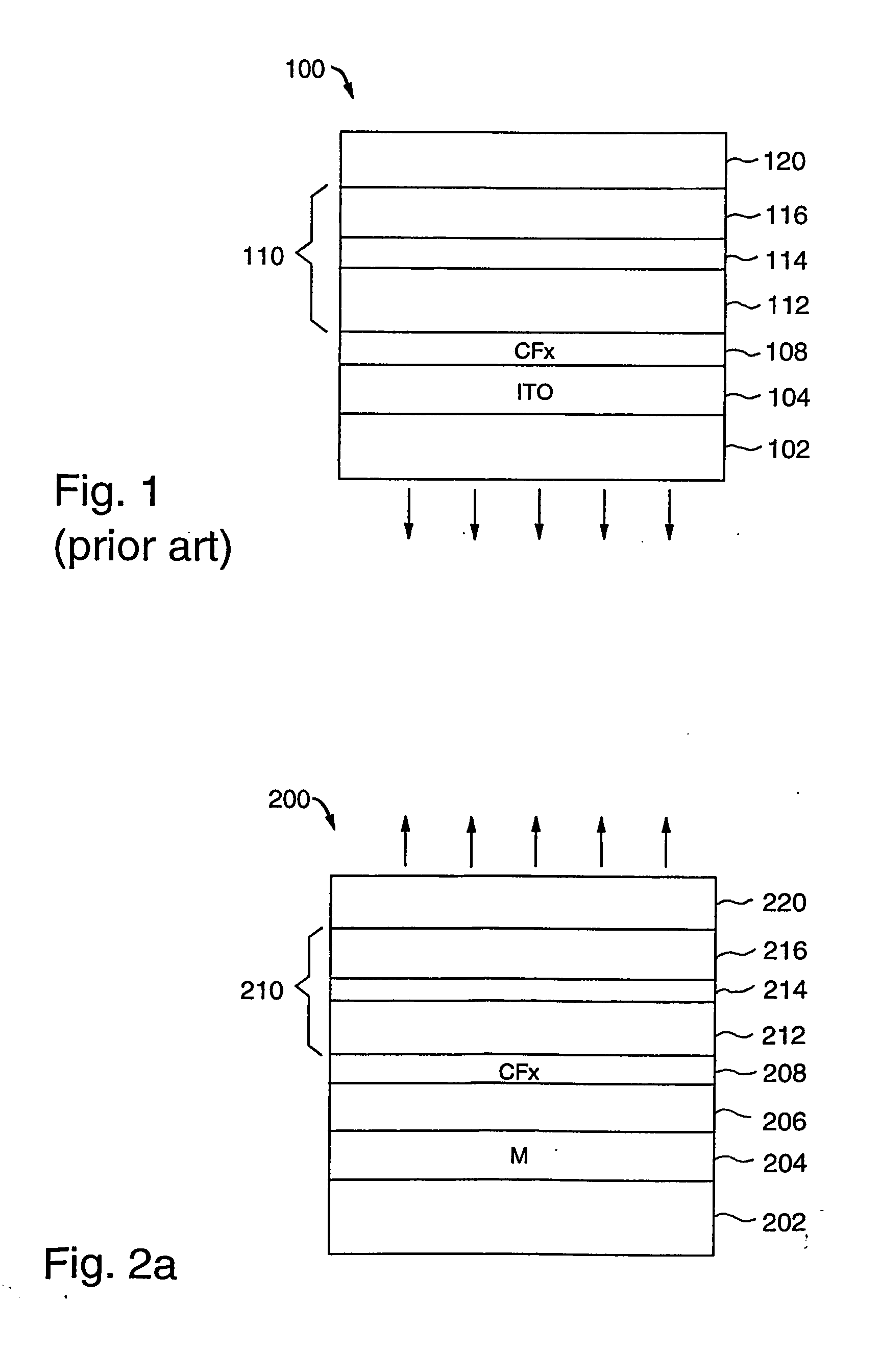
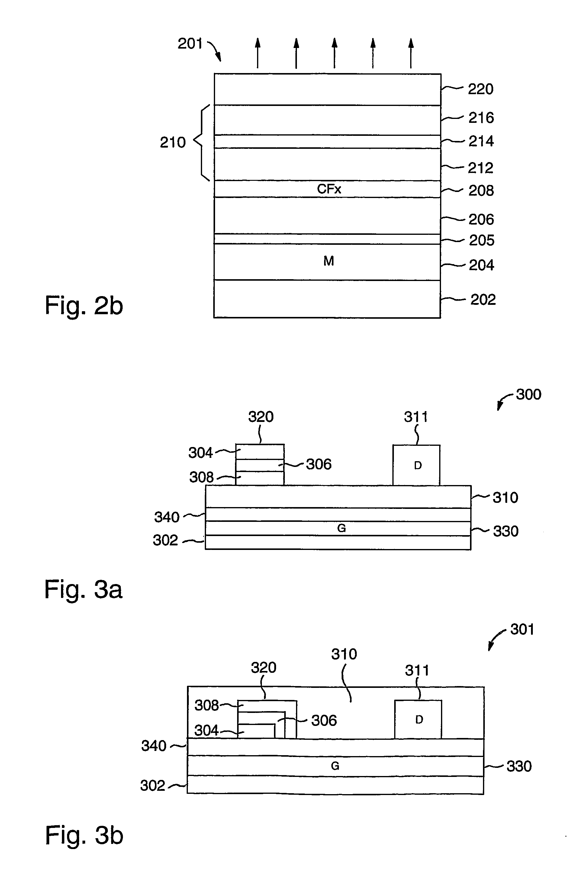
[0082] An organic light-emitting structure was constructed in the following manner: [0083] 1a) evaporation of Ti on glass (substrate) [0084] 1b) evaporation of Al on Ti / glass [0085] 1c) deposition of ITO, optional a buffer layer of Pt or Ti can be formed between Al and ITO [0086] 2) insertion of the structure in a plasma etch / deposition machine for [0087] a) oxygen plasma treatment for cleaning and oxidation (also for ITO); [0088] b) deposition of a 3 nm fluorocarbon polymer by ...


PUM

PropertyMeasurementUnit
thicknessaaaaaaaaaa
work functionaaaaaaaaaa

Abstract

The present invention discloses an electrode structure for electronic and opto-electronic devices. Such a device comprises a first electrode substantially having a conductive layer (204), a nonmetal layer (206) formed on the conductive layer, a fluorocarbon layer (208) formed on the nonmetal layer, a structure (210) formed on the structure. The electrode may further comprise a buffer layer (205) between the conductive layer and the nonmetal layer.

Description

TECHNICAL FIELD [0001] The present invention is related to an electrode design for an electronic device. More particularly the invention relates to an electrode modification for electronic and opto-electronic devices. BACKGROUND OF THE INVENTION [0002] Electronic and opto-electronic devices such as organic light-emitting diodes (OLEDs) are known in the art. Those OLEDs are also referred to as organic electroluminescent (EL) devices which generally comprise an organic electroluminescent material sandwiched between two electrodes. Generally, the organic electroluminescent material is a multilayer structure comprising an electron transport layer, an electroluminescent layer and a hole transport layer. Upon application of an electrical current, the material radiates light generated by recombination of electrons and holes in the organic material. However, the organic luminescent materials are sensitive to impurities, oxygen, and humidity. Further, in some electronic or opto-electronic de...

Claims


Application Information

Patent Timeline
Patent Type & Authority Applications(United States)
IPC IPC(8): H01L51/50H01L51/52H05B33/10H05B33/22
CPCH01L51/5088H01L2251/5315H01L51/5206H10K50/17H10K50/818H10K2102/3026
Inventor ALVARADO, SANTOS F.BEIERLEIN, TILMAN A.CORNE, BRIAN K.DRECHSLER, UTEGERMANN, ROLANDKARG, SIEGFRIED F.MUELLER, PETERRIEL, IIEIKERIESS, WALTERRUHSTALLER, BEATSEIDLER, PAULWIDMER, ROLAND
Owner GLOBALFOUNDRIES US INC
Why Eureka
Try Eureka