Electroluminescent device having a thin-film layer, and electronic device having the electroluminescent device

a technology of electroluminescent devices and thin-film layers, which is applied in the direction of discharge tube luminescnet screens, organic semiconductor devices, natural mineral layered products, etc., can solve the problems of insufficient efficiency, display may be disabled, and the luminescent color shifts toward the longer wavelength side with current-application time, so as to achieve satisfactory efficiency and improve reliability. , the effect of satisfactory efficiency

Inactive Publication Date: 2005-03-03
SEIKO EPSON CORP
View PDF16 Cites 22 Cited by
  • Summary
  • Abstract
  • Description
  • Claims
  • Application Information

AI Technical Summary

Benefits of technology

[0010] Taking the problems described above into consideration, the object of the present invention is to provide element configurations of electroluminescent devices using organic polymer materials, and more preferably, organic polymer materials for blue light emission as light-emitting materials, in which changes of luminescent color upon current application are suppressed and reliability is improved. In addition, the present invention provides element configurations capable of achieving satisfactory efficiency by suppressing unnecessary current, and provides element configurations capable of achieving satisfactory efficiency even for electroluminescent devices using organic polymer materials having wavelengths of green or longer. Furthermore, in a process for manufacturing display apparatuses by using a printing method, specifically, by using an ink-jet method, another object of the present invention is to prevent electrical short circuits at printing defects that may occur depending on the conditions.

Problems solved by technology

However, concerning organic polymer materials for blue light emission, even though the initial characteristics thereof can be satisfactory, there is the problem in that the wavelength of the luminescent color shifts toward the longer wavelength side with current-application time.
In addition, in electroluminescent devices using organic polymer materials as light-emitting materials, impurities exist therein due to difficulties in purifying organic polymers, and current which does not contribute to light emission flows through these impurities, whereby there is a problem in that sufficient efficiency cannot be obtained.
Furthermore, in a process for manufacturing electroluminescent devices, printing defects may occur when a printing method, specifically, an ink-jet method, is used as a method for forming a light-emitting layer, and electrical short circuits caused by the printing defects may occur, whereby there is a problem in that display may be disabled.

Method used


Image

  • Electroluminescent device having a thin-film layer, and electronic device having the electroluminescent device
  • Electroluminescent device having a thin-film layer, and electronic device having the electroluminescent device
  • Electroluminescent device having a thin-film layer, and electronic device having the electroluminescent device

Examples


example 1

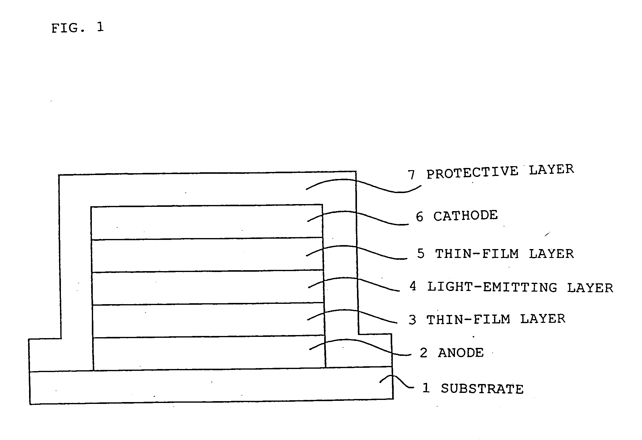
[0045] In an electroluminescent device having a structure provided with an organic polymer and disposed between two electrodes (anode and cathode), one of which is transparent, according to this Example, an example will be described in which the organic polymer emits light in the wavelength range between 400 nm to 600 nm, and a thin-film layer is disposed between the organic polymer and the cathode.

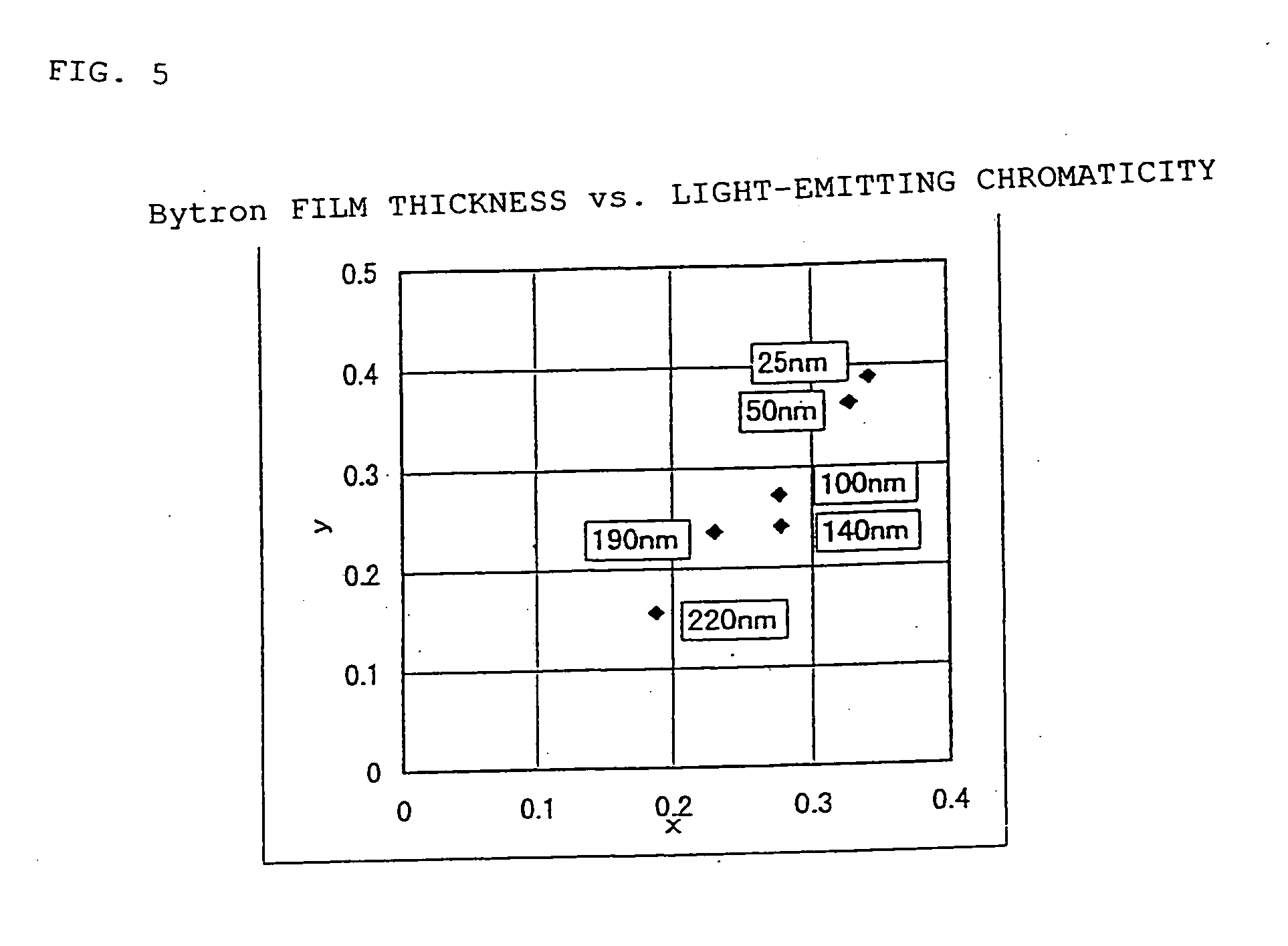
[0046] In FIG. 1, a cross-sectional view of the electroluminescent device of the present invention is shown. As a transparent electrode (anode), an indium tin oxide (ITO) film was formed on a transparent glass substrate 1 and was then patterned. Next, as a (positive) hole injection layer (transport layer) to be used as a thin-film layer 3, a 100-nm thick film composed of, for example, Bytron (Bayer AG) was formed by coating followed by drying thereof. Then, a xylene solution containing one percent of poly(dioctyl)fluorene was coated and dehydrated, and a 50-nm thick film thereof was obta...

example 2

[0058] In this Example, an example will be described, in which a fluoride or an oxide of an alkali metal; a fluoride or an oxide of an alkaline earth metal; or a fluoride or an oxide of a group III element in the periodic table, is used for the thin-film layer of the structure shown in FIG. 1.

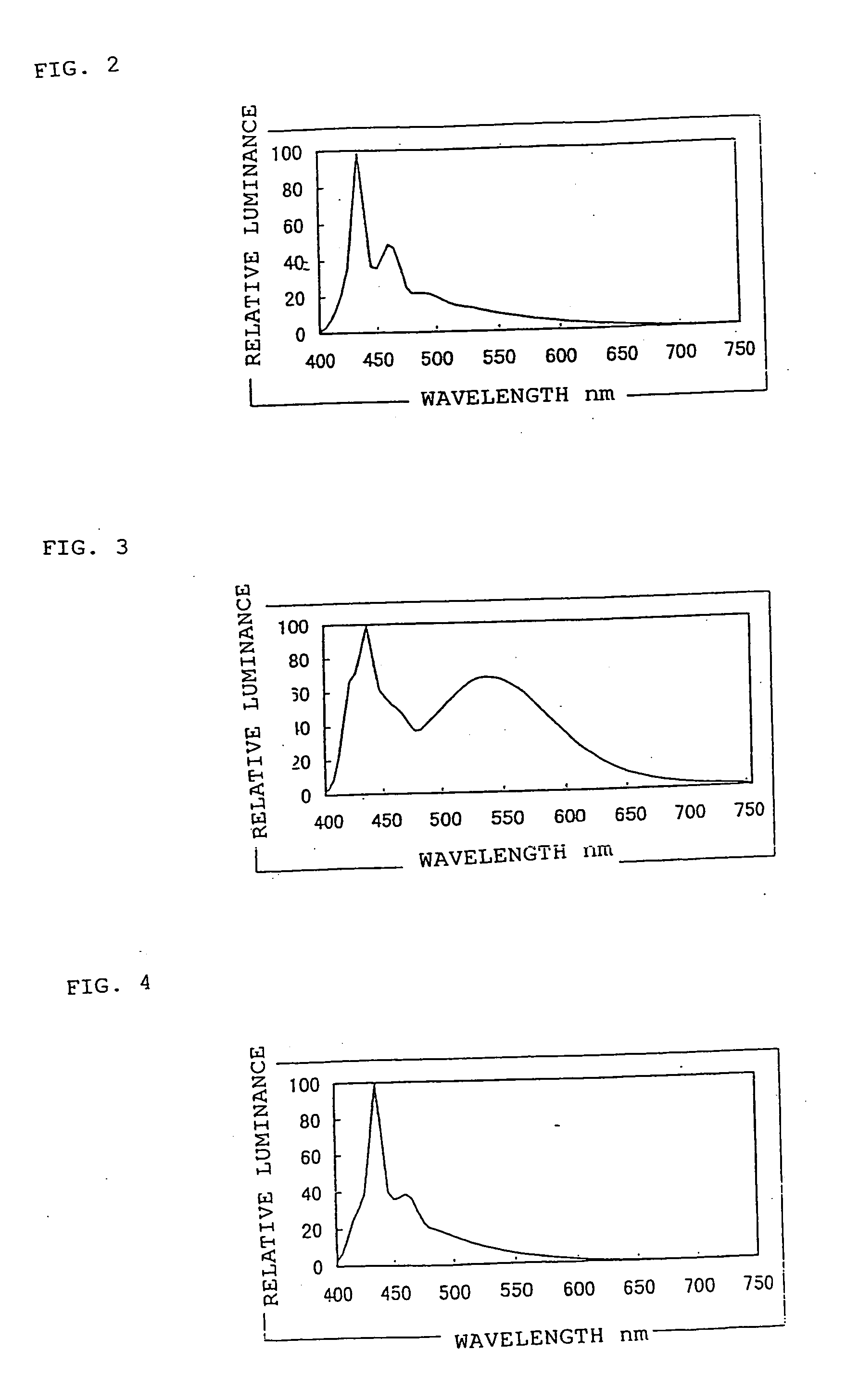
[0059] Formation methods for layers other than the thin-film layer were the same as described in Example 1. As the thin-film layer 5, calcium fluoride film formed by deposition to a thickness of 2 nm was used. The light emission spectrum of the light-emitting device (blue light-emitting device) thus prepared is shown in FIG. 4. The light-emitting efficiency was 0.17 lm / W.

[0060] In this example, calcium fluoride was used by deposition as the thin-film layer; however, lithium fluoride may also be used. In addition, a fluoride or an oxide of an alkali metal, such as lithium, sodium, or potassium; a fluoride or an oxide of an alkaline earth metal, such as beryllium, magnesium, calcium, or scandiu...

example 3

[0061] In this Example, an example will be described in which poly(p-phenylenevinylene) or a derivative thereof is used as an organic polymer for the light-emitting layer. The structure of the Example other than an organic polymer layer (light-emitting layer) was equivalent to that of the light-emitting device described in Example 1.

[0062] As the light-emitting layer 4 (layer composed of, for example, an organic polymer) in FIG. 1, precursors of poly(p-phenylenevinylene) were coated and baked, and a 100-nm thick film was thereby obtained.

[0063] The light-emitting efficiency of the electroluminescent device thus prepared was 1.16 lm / W.


PUM

PropertyMeasurementUnit
wavelength rangeaaaaaaaaaa
thicknessaaaaaaaaaa
thicknessaaaaaaaaaa

Abstract

The invention provides an electroluminescent device having a structure that may include a light-emitting layer composed of, for example, at least an organic polymer between an anode and a cathode, and may also include a thin-film layer disposed between the light-emitting layer and the cathode, the thin-film layer suppressing unnecessary current which does not contribute to light emission.

Description

[0001] This is a Continuation of application Ser. No. 09 / 509,121 filed Mar. 23, 2000, which is the National Stage of International Application No. PCT / JP99 / 03978 filed Jul. 23, 1999. The disclosure of the prior applications are hereby incorporated by reference herein in their entirety.BACKGROUND OF THE INVENTION [0002] 1. Field of Invention [0003] The present invention relates to structures of electroluminescent devices used for terminal components of information apparatuses, such as displays. [0004] 2. Description of Related Art [0005] Among recent aggressive activities for developing next generation luminous displays to replace cathode ray tubes (CRT) and liquid crystal displays, research and development of plasma display panels (PDP), field-emission displays (FED), organic electroluminescent displays have been actively performed. In organic electroluminescent materials, organic polymer materials emitting blue, green, and orange light, have been developed to such a level that the ...

Claims


Application Information

Patent Timeline
Patent Type & Authority Applications(United States)
IPC IPC(8): H01L27/32C09K11/06H01L51/50H01L51/52H05B33/10H05B33/12H05B33/14H05B33/22
CPCH01L27/3295H01L51/5012H05B33/22H01L51/5092H01L2251/558H01L51/5088H10K59/122H10K59/173H10K50/11H10K50/17H10K50/171H10K2102/351
Inventor KOBAYASHI, HIDEKAZU
Owner SEIKO EPSON CORP
Why Eureka
Try Eureka