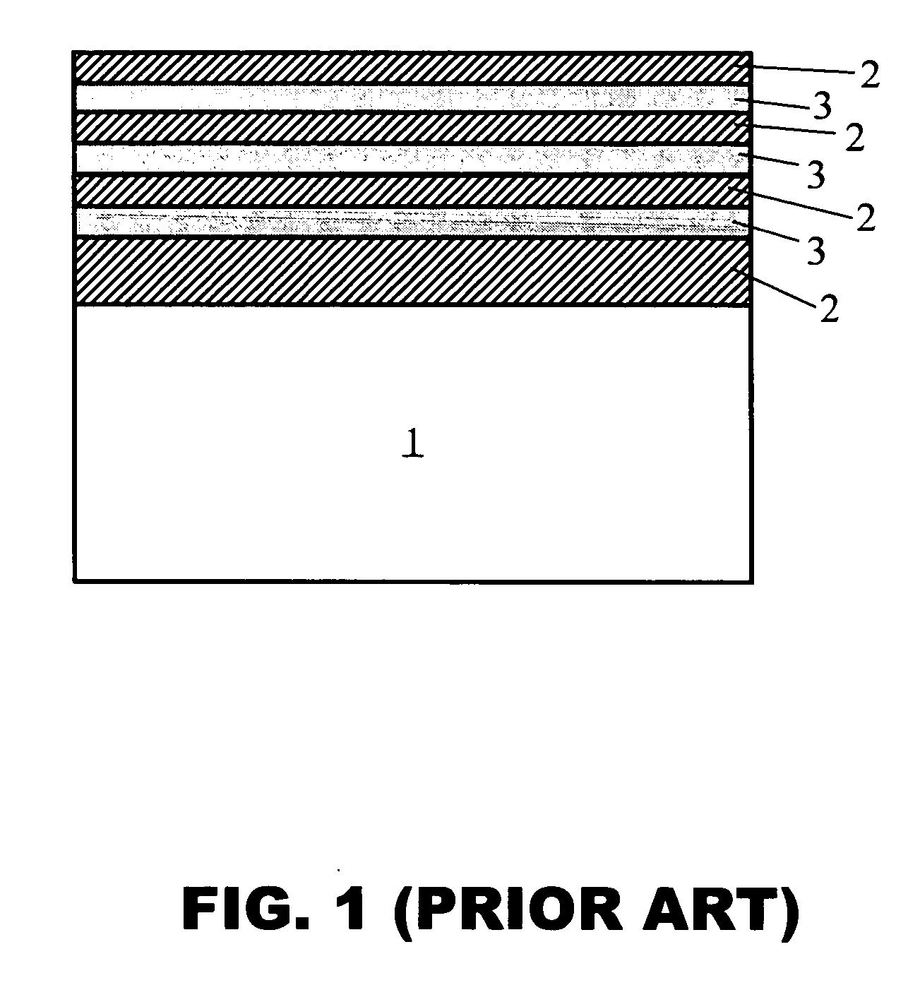
[0016] Another key
advantage of the present invention, over the
solid continuous inorganic layers of prior art barrier structures, is the much higher
toughness and fracture-resistance provided by the
polymer infiltrated porous material, since the infiltrated
polymer provides both greater flexibility to the IPBM, as well as greater resistance to
fracture propagation. Accordingly, the presently disclosed barrier is seen as particularly well-suited to applications using flexible substrates.
[0017] Another
advantage of the presently disclosed barrier structure is the relatively robust and inexpensive
processing required for its fabrication, relative to the highly controlled
processing required for achieving the substantially continuous inorganic layers of previous multilayer barriers. The novel infiltrated porous barrier material (IPBM) of the present invention can thus be substituted for the relatively rigid and dense inorganic barrier layers utilized in any multilayer barrier structure of the prior art.
[0018] In one preferred embodiment of the disclosed barrier, the function of the barrier is to prevent environmental constituents including but not limited to water,
oxygen and combinations thereof from reaching the
OLED device. Accordingly the invention is a method for preventing water or
oxygen from a source thereof reaching an electronic device. Due to the novel properties of the disclosed IPBM layer—in particular, the characteristics of both an effective permeation barrier combined with those of a relatively flexible material—it may be found advantageous to substitute the disclosed IPBM for either the organic or inorganic layers used for barrier properties in prior art
OLED structures. Alternatively, the IPBM of the present disclosure may be interleaved with the existing barrier materials of the prior art OLED devices. There are numerous OLED devices that incorporate a barrier structure in the prior art, many of which teach barrier multilayers comprising distinct layers of transparent
inorganic materials alternating with distinct layers of transparent polymers. Such OLED devices are disclosed in numerous references, including U.S. Pat. No. 6,503,634, U.S. Pat. No. 6,503,634, U.S. Pat. No. 05,686,360, U.S. Pat. No. 05,757,126, U.S. Pat. No. 05,757,126, U.S. Pat. No. 06,413,645, U.S. Pat. No. 06,413,645, U.S. Pat. No. 06,497,598, U.S. Pat. No. 06,497,598, and various referenced and referencing patents of these disclosures, as well as the following US patent applications: US200030124392, US200030124392. Accordingly, in any of these prior art OLED barrier structures, the dyad of both
polymer layer and
inorganic layer, the inorganic layer alone, or the polymer layer alone, may optionally be substituted by the IPBM layer of the present invention. It may also be seen that the inorganic transparent conductors (e.g, ITO,
zinc oxide,
magnesium oxide, etc) may be utilized to form the porous inorganic layer of the present invention. Conversely, conducting polymers (e.g.,
polyaniline, polypyrole, etc) might be used as the infiltrated organic material.
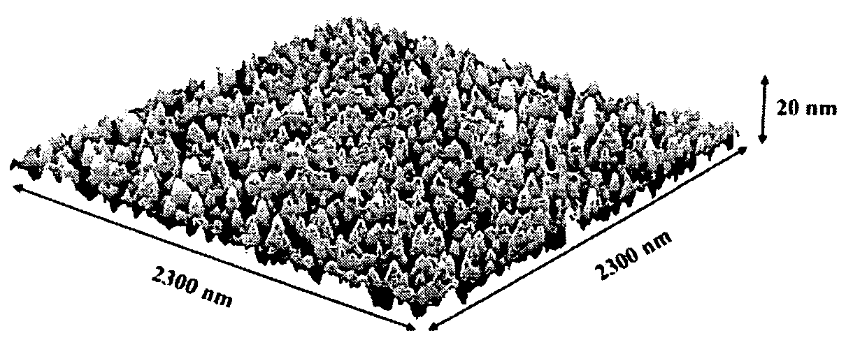
[0019] As is common in the materials sciences, the terms “pore” and “porous” will, in the present disclosure, refer to the characteristic of a material to posses microscopic voids, wherein the voids possess substantially lower
material density than surrounding material. Thus,
porosity does not specify a particular characteristic shape of the voids, only the degree to which fillable voids exist. Accordingly, the degree of
porosity is ascertained in the prior art, and in the present disclosure, by the amount of a particular substance that may be consumed in filling the pores of a
unit volume of the porous material. Also, the terms “nanophase” and “
nanoporous” are used in the present disclosure to describe material properties that are utilized in the preferred embodiments. Whereas the present invention is not limited to such dimensional restraints, the terms “nanophase”, “
nanoporous”, and nanoscale, will refer, as in previous work in the
nanomaterials field, to materials wherein the heterogeneity in question has a spatial dimension on the order of less than a micron. The term “compound” or “compounds” refers herein, as it does in the prior art of materials sciences and
engineering, to a material formed by the reaction of at least two elements. Accordingly, all oxides, nitrides, fluorides, carbides, borides, phosphates, sulfates, silicates, selenides, lanthanides, cuprates, cobaltites, magnatites, tellurides, arsenates, various
intermetallic compounds, and any other such reacted material, is included in this definition.
[0021] One object of the invention is to provide a multilayer barrier structure that may be economically fabricated on a
commercial scale.
[0022] Yet, another object of the invention is to provide an IPBM layer that possesses desired properties of both glass and polymer layers.

