
Diamond triode devices with a diamond microtip emitter

a diamond triode and emitter technology, applied in the field of vacuum microelectronics, can solve the problems of unsatisfactory emission performance, unsatisfactory potential, non-uniform diamond coated silicon tips, etc., and achieve the effect of enhancing the emission performance of the structure, ideal or controllable balance of emission efficiency and durability

Inactive Publication Date: 2005-03-24
VANDERBILT UNIV
View PDF2 Cites 13 Cited by
  • Summary
  • Abstract
  • Description
  • Claims
  • Application Information

AI Technical Summary

Benefits of technology

[0011] The novel fabrication processes of this invention include the ability to control the carbon graphite content of the diamond. This produces a diamond tip with an ideal or controllable balance of emission efficiency and durability. Emission performance of the structure is further enhanced by vacuum-thermal-electric treatment of the tips, hydrogen plasma tip sharpening, high temperature annealing, and application of thin metal coatings to the tips.

Problems solved by technology

However, due to the chemical inertness of diamond, the work reported in the prior art involves only planar diamond films, non-uniformly diamond coated silicon tips, or irregular ion-etched diamond conical structures.
Although those skilled in the art have recognized that diamond has properties that make it potentially very useful as an emitter in microelectronic devices, that potential has remained unfulfilled up to now.
Various emitter structures using diamond have been designed but their emission performance has been unsatisfactory.
For example, many prior art diamond tipped emitter structures have been inefficient emitters or have produced emission currents that are unstable.
In those few instances in the prior art where efficient and stable diamond tip emitters have been built, the fabrication techniques have been expensive and / or time consuming.
Although the diamond coating may enhance the emission characteristics of the emitter (assuming that the device could actually be built as described), the device will not have the same desirable characteristics found in a solid, monolithic diamond emitter structure.

Method used


Image

  • Diamond triode devices with a diamond microtip emitter
  • Diamond triode devices with a diamond microtip emitter
  • Diamond triode devices with a diamond microtip emitter

Examples


second embodiment

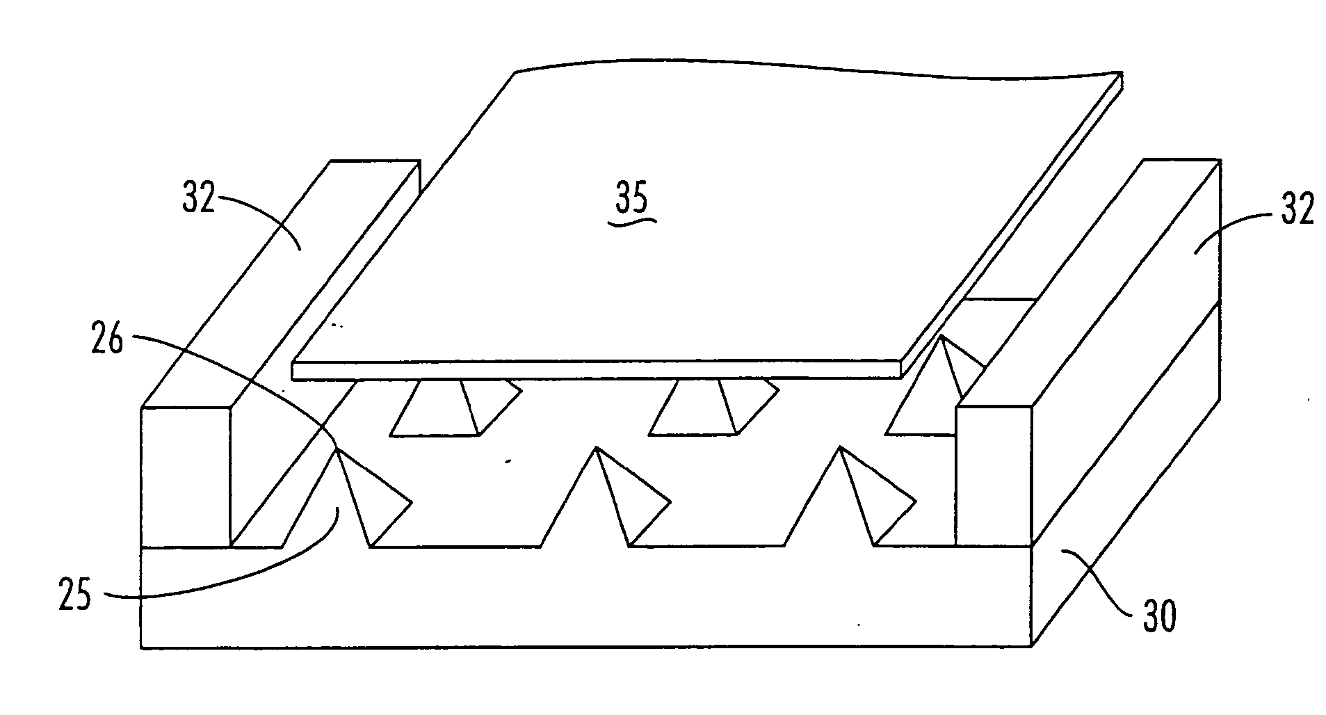
[0178]FIG. 26 is a diamond diode pressure sensor utilizing a conducting gate or anode 35, an insulator 40, and a pyramidal diamond microtip emitter 25 (as a cathode) on a flexible diamond substrate 30.

third embodiment

[0179]FIG. 27 shows a diamond diode pressure sensor utilizing a pyramidal diamond microtip emitter 25 on a diamond substrate 30, an insulating layer 40, and a flexible diamond diaphragm as the anode 35. In the embodiment of FIG. 27, the anode 35 will move toward or away from the emitter 25 in response to pressure changes outside the chamber 38.

[0180] The pressure sensor of FIG. 28 uses a diamond vacuum triode device, having a diamond microtip emitter 25 on a diamond substrate 30, a grid 45 supported above the substrate 30 by a first insulating layer 41, and a flexible diaphragm (diamond, for example) as an anode 35, supported by a second insulating layer 40.

[0181]FIG. 29 illustrates an arrangement of a pyramidal diamond microtip emitter 25 as diode accelerometer device. One end of a flexible diamond substrate 30 is suspended in cantilever fashion from an insulator 40 that extends upwardly from an anode 35. If the device is subjected to a change in velocity, the substrate will flex,...


PUM


Abstract

Diamond microtip field emitters are used in triode vacuum microelectronic devices, sensors and displays. Diamond triode devices having integral anode and grid structures can be fabricated. Ultra-sharp tips are formed on the emitters in a fabrication process in which diamond is deposited into mold cavities in a two-step deposition sequence. During deposition of the diamond, the carbon graphite content is carefully controlled to enhance emission performance. The tips or the emitters are treated by post-fabrication processes to further enhance performance.

Description

CROSS-REFERENCES TO RELATED APPLICATIONS [0001] This application is a divisional application which claims benefit of co-pending U.S. patent application Ser. No. 09 / 617,531, entitled “Diamond Diode Devices with a Diamond Microtip Emitter” which is hereby incorporated by reference.[0002] A portion of the disclosure of this patent document contains material that is subject to copyright protection. The copyright owner has no objection to the facsimile reproduction by anyone of the patent document or the patent disclosure, as it appears in the U.S. Patent and Trademark Office patent file or records, but otherwise reserves all copyright rights whatsoever. STATEMENT REGARDING FEDERALLY SPONSORED RESEARCH OR DEVELOPMENT [0003] Not Applicable REFERENCE TO SEQUENCE LISTING OR COMPUTER PROGRAM LISTING APPENDIX [0004] Not Applicable BACKGROUND OF THE INVENTION [0005] The present invention relates to vacuum microelectronics and particularly to micro-patterned, microtip emitter structures made fr...

Claims


Application Information

Patent Timeline
IPC IPC(8): G01L9/00G01P15/08H01J1/30H01J1/304H01J3/02H01J9/02H01J19/02H01J19/24H01J31/12
CPCB82Y10/00G01L9/0041G01P15/0802G01P15/0894H01J1/3042G01L9/0047H01J3/022H01J9/025H01J31/127H01J2201/30407H01J2201/30457H01J1/3044G01P2015/0828
Inventor DAVIDSON, JIMMY L.KANG, WANG POOKERNS, DAVID V.HOWELL, MICKEY EVANS
Owner VANDERBILT UNIV
Learn More