Method To Reduce Stacking Fault Nucleation Sites And Reduce Forward Voltage Drift In Bipolar Devices

a bipolar device and stacking fault technology, applied in the direction of cleaning process and apparatus, semiconductor devices, chemistry apparatus and processes, etc., can solve the problems of difficult growth into large single crystals, difficult to produce silicon carbide, and high melting point of silicon carbide, so as to reduce the number of subsurface defects, reduce the number of stacking fault nucleation, and reduce the number of forward voltage drift

Active Publication Date: 2005-03-24
CREE INC
View PDF29 Cites 57 Cited by
  • Summary
  • Abstract
  • Description
  • Claims
  • Application Information

AI Technical Summary

Benefits of technology

[0025] The invention is a method of preparing a substrate for reducing stacking fault nucleation and reducing forward voltage (Vf) drift in silicon carbide-based bipolar devices. The method includes the steps of conducting a first non-selective etch on the surface of a silicon carbide substrate to remove both surface and subsurface damage; thereafter conducting a selective etch on the same surface sufficient to delineate the intersection of basal plane dislocations with the wafer surface and that will thereafter tend to propagate into epilayers as threading defects while avoiding creating beta (3C) inclusions and carrot defects; growing an epitaxial layer on the selectively etched substrate surface to a thickness greater than that of the typical thread...

Problems solved by technology

In particular, silicon carbide has an extremely high melting point and is one of the hardest known materials in the world.
Because of its physical properties, however, silicon carbide is also relatively difficult to produce.
Because silicon carbide can grow in many polytypes, it is difficult to grow into large single crystals.
The high temperatures required to grow silicon carbide also make control of impurity levels (including doping) relatively difficult, and likewise raise difficulties in the production of thin films (e.g. epitaxial layers).
Because of its hardness, the traditional steps of slicing and polishing semiconductor wafers are more difficult with silicon carbide.
Similarly, its resistance to chemical attack make it difficult to etch in conventional fashion.
As a result, growing single crystal substrates and high quality epitaxial layers (“epilayers”) in silicon carbide has been, and remains, a difficult task.
For a number of reasons, such functional problems in semiconductor devices can often result from defects in the crystal structure of the material from which the devices are formed.
In silicon carbide power devices, the availability of such relatively low-energy intermediate state encourages faults to continue to grow as the opera...

Method used


Image

  • Method To Reduce Stacking Fault Nucleation Sites And Reduce Forward Voltage Drift In Bipolar Devices
  • Method To Reduce Stacking Fault Nucleation Sites And Reduce Forward Voltage Drift In Bipolar Devices
  • Method To Reduce Stacking Fault Nucleation Sites And Reduce Forward Voltage Drift In Bipolar Devices

Examples


Embodiment Construction

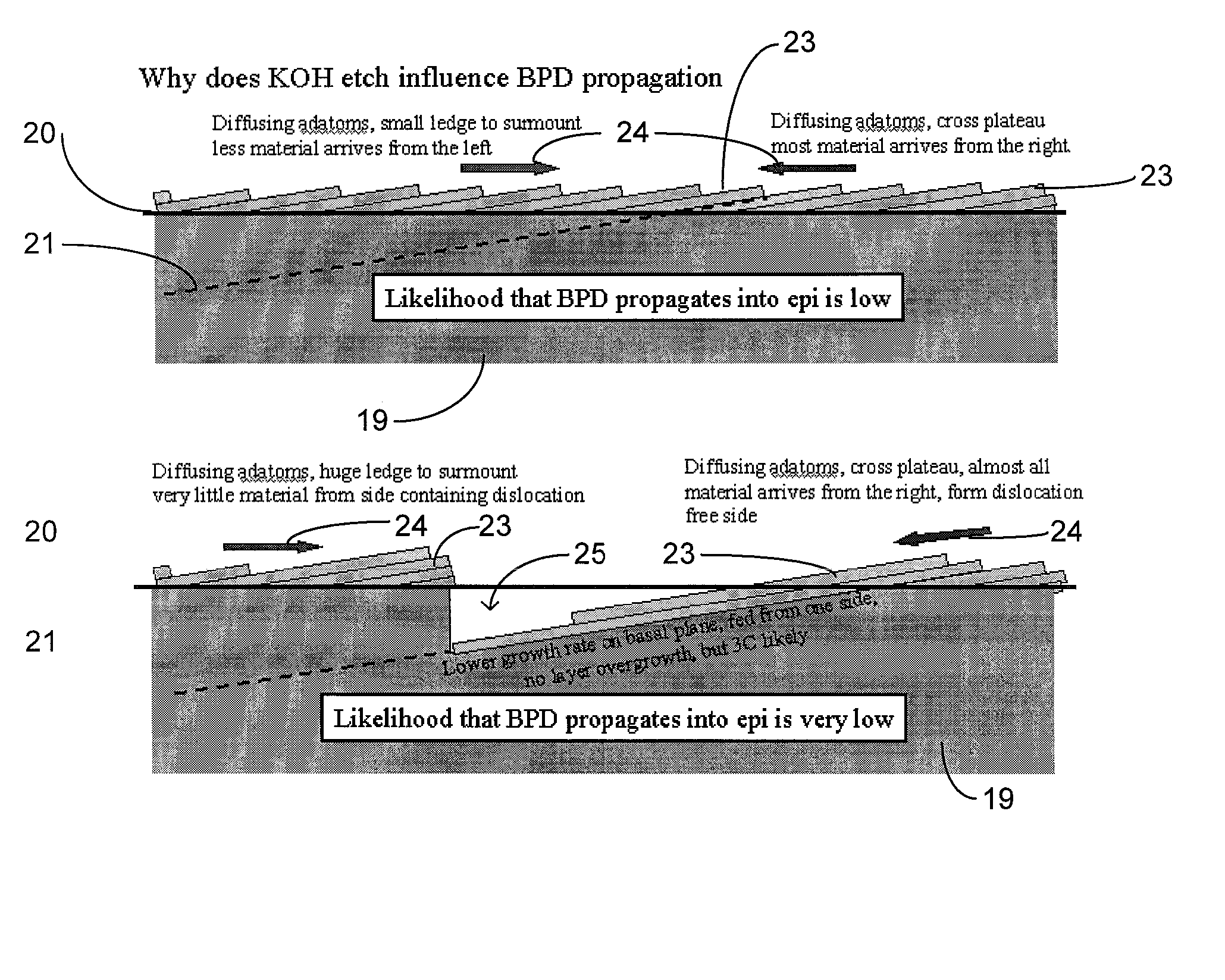
[0033] The invention is a method of preparing a substrate for reducing stacking fault nucleation and reducing forward voltage (Vf) drift in silicon carbide-based bipolar devices.

[0034] In a first embodiment the method initially comprises conducting a non-selective etch, preferably a dry etch, most preferably a reactive ion etch (RIE), on the surface of a silicon carbide substrate to remove both surface and sub-surface damage that typically results from the sawing and lapping of the extremely hard SiC material. As known to those familiar with the manufacture of electronic devices, a nonselective etch removes all material at an equal rate. A selective etch removes specific materialse.g. damaged, n-type, p-typemore quickly than the other materials. Exemplary, but not limiting, techniques for dry etching of silicon carbide are set forth in U.S. Pat. No. 4,865,685 and its sibling U.S. Pat. No. 4,981,551 the contents of which are incorporated entirely herein by reference. Other technique...


PUM

PropertyMeasurementUnit
Electric chargeaaaaaaaaaa
Electrical conductivityaaaaaaaaaa
Electrical conductoraaaaaaaaaa

Abstract

A method is disclosed for preparing a substrate and epilayer for reducing stacking fault nucleation and reducing forward voltage (Vf) drift in silicon carbide-based bipolar devices. The method includes the steps of etching the surface of a silicon carbide substrate with a nonselective etch to remove both surface and sub-surface damage, thereafter etching the same surface with a selective etch to thereby develop etch-generated structures from at least any basal plane dislocation reaching the substrate surface that will thereafter tend to either terminate or propagate as threading defects during subsequent epilayer growth on the substrate surface, and thereafter growing a first epitaxial layer of silicon carbide on the twice-etched surface.

Description

FEDERAL RESEARCH STATEMENT [0001] This invention was developed under government contract No. N00014-02-C-0302. The U.S. Government has a paid-up license in this invention and the right in limited circumstances to require the patent owner to license others on reasonable terms as provided for by the terms of contract No. N00014-02-C-0302 awarded by the Defense Advanced Research Projects Agency (“DARPA”).BACKGROUND OF INVENTION [0002] The present invention relates to increasing the quality and desired properties of semiconductor materials used in electronic devices, particularly power electronic devices. In particular, the invention relates to an improved process for minimizing crystal defects in silicon carbide, and the resulting improved structures and devices. The present invention is related to the subject matter disclosed and claimed in co-pending and commonly assigned application Ser. No. 10 / 046,346; filed Oct. 26, 2001 and now published as No. 2003-0080842 A1; the contents of wh...

Claims


Application Information

Patent Timeline
IPC IPC(8): H01L21/20H01L21/205
CPCY10S438/931H01L21/30608H01L21/3065H01L21/02658H01L21/02378H01L21/02529H01L21/02019
Inventor SUMAKERIS, JOSEPH JOHN
Owner CREE INC
Why Eureka
Try Eureka