Optical semiconductor device

a technology of optical semiconductors and semiconductor modules, applied in the direction of lasers, electromagnetic transceivers, semiconductor lasers, etc., can solve the problems of no margin at all to the prescription of eye masks, oscillation frequency, conspicuous deterioration of optical output waveforms of ld modules, etc., to improve the waviness of frequency response characteristics

Inactive Publication Date: 2005-03-31
MITSUBISHI ELECTRIC CORP
View PDF12 Cites 19 Cited by
  • Summary
  • Abstract
  • Description
  • Claims
  • Application Information

AI Technical Summary

Benefits of technology

[0043] According to the present invention, at least two bias circuits having asymmetric impedances can constitute the semiconductor optical modulation device which improves a waviness of frequency response characteristics.

Problems solved by technology

Nevertheless, if a modulated signal at 10 Gb / s or more is to be transmitted, the optical output waveform of the LD module is conspicuously deteriorated as shown in FIG. 20.
However, the eye mask margin is quite small near an upper right part of the central portion (a rising part indicated by W2 in FIG. 20), with the result there is no margin at all to the eye mask prescription.
Therefore, a problem occurs that if, for example, a surrounding temperature rises, a relaxation oscillation frequency of the optical semiconductor falls and the signal waveform cannot satisfy the upper right part of the central portion of the eye mask.
As a result, the transmission characteristics of the optical signal to be output are deteriorated.
This results in quite sharp damping characteristics.
As can be seen, the conventional optical semiconductor device has problems that output characteristics of the optical signal is influenced by poor fall characteristics of the LD driving circuit and the transmission characteristics of the optical signal is thereby deteriorated.
Further, the conventional optical semiconductor device has a problem that passing characteristics of the LD module suddenly attenuates at the frequency near 10 gigahertz.
The sharp decline of the characteristics near 10 gigahertz particularly causes the great deterioration of the optical output waveform of the optical semiconductor device.

Method used


Image

  • Optical semiconductor device
  • Optical semiconductor device
  • Optical semiconductor device

Examples


first embodiment

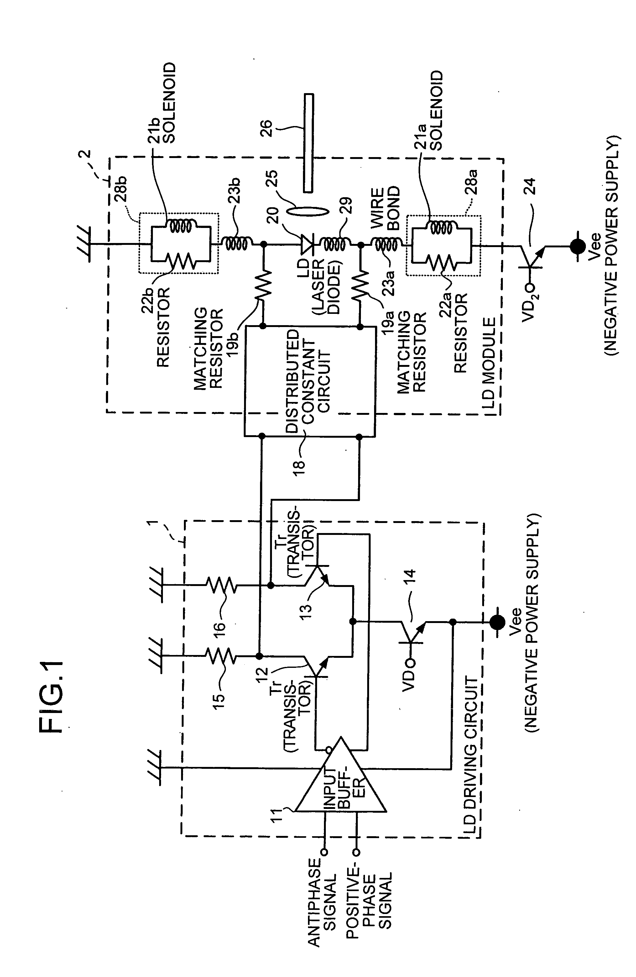
[0080]FIG. 1 is a circuit block diagram which illustrates one example of an optical semiconductor device according to the first embodiment. In FIG. 1, an LD driving circuit 1 includes an input buffer 11 which has a differential input configuration, a pair of differential transistors 12 and 13 which have differential configuration and which output an antiphase signal and a positive phase signal, respectively, a transistor 14 which performs a constant-current operation, and resistors 15 and 16 which are loads of collectors of the differential transistors 12 and 13, respectively, and which make impedance matching.

[0081] The input buffer 11 shapes waveforms of input antiphase signal and positive phase signal, and generates the adjusted antiphase signal and positive phase signal to be input to bases of the differential transistors 12 and 13.

[0082] The paired differential transistors 12 and 13 that have the differential configuration and the transistor 14 constitute a differential ampli...

second embodiment

[0116]FIG. 5 is a circuit block diagram which illustrates one example of the optical semiconductor device in the second embodiment. In FIG. 5, the LD driving circuit 1 includes the input buffer 11 which has differential input configuration, the paired differential transistors 12 and 13 which have differential configuration to output an antiphase signal and a positive phase signal, respectively, the transistor 14 which performs a constant-current operation, and the resistors 15 and 16 which are resistors against the loads of collectors of the differential transistors 12 and 13, respectively,,and which make impedance matching.

[0117] The input buffer 11 shapes waveforms of input antiphase signal and positive phase signal, and generates the adjusted antiphase signal and positive phase signal to be input to bases of the differential transistors 12 and 13.

[0118] The paired differential transistors 12 and 13 that have the differential configuration and the transistor 14 constitute a diff...

third embodiment

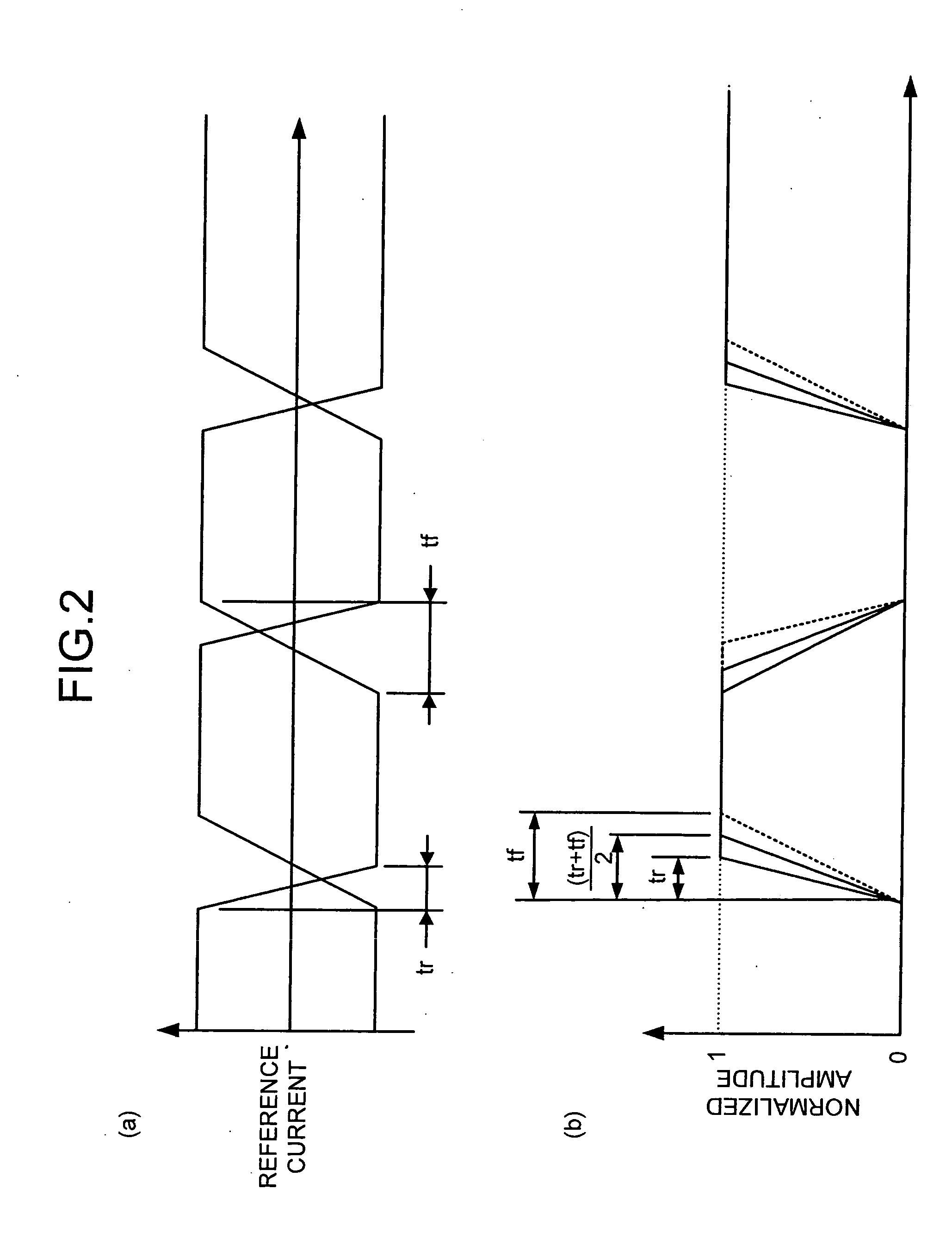
[0136] In the first embodiment, the advantages of using the differential lines have been explained while centering around the advantage of compensating the asymmetry of the rise / fall characteristics of the LD driving circuit and improving the optical output waveform. By employing the differential lines, there is an advantage in that frequency characteristics can be improved besides the advantage of compensating the asymmetry of the rise and fall characteristics. In this embodiment, the advantage of improving the frequency characteristics will be explained while referring to equivalent circuits for specific examples of reactances and resistances.

[0137]FIG. 9(a) is a simplified equivalent circuit diagram which simulates a high frequency operation of the conventional optical semiconductor device shown in FIG. 18. In FIG. 9(a), reference symbol 31 denotes the output impedance of the LD driving circuit, 309 denotes a matching resistor, and 310 denotes the internal resistance of the LD. ...


PUM


Abstract

The present invention includes a first conductor line connected to one end of an optical semiconductor element (20), and supplying an electric signal to this optical semiconductor element (20); a second conductor line connected to the other end of the optical semiconductor element (20), and supplying an electric signal to this optical semiconductor element (20); a first inductance element (21a) connected to the one end of the optical semiconductor element (20), and cutting off the electric signal at a high frequency; and a second inductance element (21b) connected to the other end of the optical semiconductor element (20), and cutting off the electric signal at the high frequency, wherein the first and the second conductor lines constitute differential lines.

Description

TECHNICAL FIELD [0001] The present invention relates to an optical semiconductor device including an optical semiconductor element that outputs an optical signal modulated based on an electric signal. BACKGROUND ART [0002]FIG. 18 is a circuit diagram which illustrates one example of a conventional single-phase feed type optical semiconductor device. Circuits similar to such a circuit are disclosed by, for example, Japanese Patent Application Laid-Open Publication Nos. 9-200150 and 8-172401. [0003] In the optical semiconductor device shown in FIG. 18, an LD driving circuit 200 that drives a semiconductor laser diode element 310 (hereinafter, “LD”) is connected to an LD module 300. A light emission output of the LD 310 is output from an optical fiber 316. Differential transistors 202 and 203, which constitute a differential amplifier are driven by a constant current by a transistor 204, are applied with complementary data input signals (a positive phase signal and an antiphase signal)...

Claims


Application Information

Patent Timeline
Patent Type & Authority Applications(United States)
IPC IPC(8): H01L23/48H01L23/52H01L29/40H01S5/022H01S5/042H04B10/07H04B10/2507H04B10/40H04B10/50H04B10/60
CPCH01S5/02212H01S5/02216H01S5/02248H01S5/02284H01S5/0427H01L2924/19107H01S5/06226H01L2224/48091H01L2924/00014H01S5/02325H01S5/02251
Inventor ARUGA, HIROSHIKANEKO, SHINICHISAKAI, KIYOHIDE
Owner MITSUBISHI ELECTRIC CORP
Why Eureka
Try Eureka