Apparatus and method for photovoltaic energy production based on internal charge emission in a solid-state heterostructure

a photovoltaic energy and heterostructure technology, applied in the field of photovoltaic cells, can solve the problems of limited material and device structure, high manufacturing cost, and inability to meet the requirements of cells, and achieve the effect of promoting the longevity of solar cells and increasing the longevity of solar cell devices

Inactive Publication Date: 2005-04-28
ADRENA
View PDF10 Cites 21 Cited by
  • Summary
  • Abstract
  • Description
  • Claims
  • Application Information

AI Technical Summary

Benefits of technology

[0017] In is yet another object of the present invention to increase the longevity of the solar cell devices by using stable components. In the case of photoelectrochemical cells, most types of feasible electrolytes are reactive and can erode or dissolve the adjacent semiconductor or react with the dye, causing the device to be unstable. By eliminating the need to use reactive components, the present invention promotes the longevity of solar cells.

Problems solved by technology

Gallium arsenide cells are among the most efficient solar cells available today, with many other advantages, however they are also expensive to manufacture.
Conventionally, expensive material and device structures are required to achieve cells that provide both high efficiency and low recombination probability and leakage.
However, defect free, thick, narrow band-gap, materials are limited in numbers and expensive to fabricate.
In heterostructures a limited number of acceptable compatible materials are available.
This device is limited in its power output by the relative free energies of electrons in the electrolyte and the semiconductor which limit the photovoltage.
Additional inefficiencies result from the required molecular diffusion of the donors to the electrode as well as overpotential losses at the electrode / electrolyte interface.
However, as previously mentioned, neither patent suggests the physical properties of the reducing agent, and it is unclear whether the proposed devices disclosed in the '470 and '950 patents can indeed yield the purported results.
An implementation of the device was published using an organic hole transport material, however, the performance and longevity were poor [ref: U. Bach, et al., Nature, Vol. 395, October 1998, pg.

Method used


Image

  • Apparatus and method for photovoltaic energy production based on internal charge emission in a solid-state heterostructure
  • Apparatus and method for photovoltaic energy production based on internal charge emission in a solid-state heterostructure
  • Apparatus and method for photovoltaic energy production based on internal charge emission in a solid-state heterostructure

Examples


Embodiment Construction

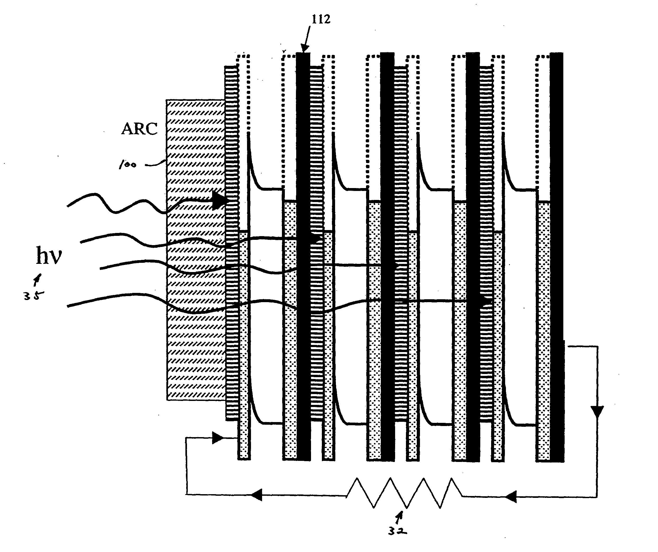
[0037] Various embodiments of the present invention will be described with reference to FIGS. 3-11. Although only a limited number of embodiments of the invention are described hereinafter, it shall be understood that the detailed discussion of the embodiments is not intended to limit the present invention to those particular embodiments.

[0038]FIG. 3 illustrates a photosensitized solid-state device in accordance with the preferred embodiment of the present invention. More specifically, the photosensitized solid-state device includes a photosensitive layer 10, a front conducting layer 31, a charge separation layer 39, a back conducting layer 30, and a load 32. The front conducting layer 31 is preferably an ultra-thin metal film (preferably in the nanometer range), while the back conducting layer 30 is preferably an ohmic conducting layer. The charge separation layer 39 has a determinable conduction band energy level 38 and a determinable valence band energy level 37. In an alternati...


PUM

PropertyMeasurementUnit
thicknessaaaaaaaaaa
band gapaaaaaaaaaa
thicknessaaaaaaaaaa

Abstract

An apparatus and method for solar energy production comprises a multi-layer solid-state structure including a photosensitive layer, a thin conductor, a charge separation layer, and a back ohmic conductor, wherein light absorption occurs in a photosensitive layer and the charge carriers produced thereby are transported through the thin conductor through the adjacent potential energy barrier. The open circuit voltage of the solar cell can be manipulated by choosing from among a wide selection of materials making up the thin conductor, the charge separation layer, and the back ohmic layer.

Description

[0001] The present invention is directed to low cost, high efficiency solar cell technology. More specifically, the present invention is related to a method and apparatus for producing photovoltaic energy using solid-state devices. BACKGROUND OF THE INVENTION [0002] Conventional photovoltaic cells convert sunlight directly into electricity by the interaction of photons and electrons within the semiconductor material. Most solid-state photovoltaic devices rely on light energy conversion to excite charge carriers (electrons and holes) within a semiconductor material and charge separation by a semiconductor junction producing a potential energy barrier. To create a typical photovoltaic cell, a material such as silicon is doped with atoms from an element with one more or less electrons than occurs in its matching substrate (e.g., silicon). A thin layer of each material is joined to form a junction. Photons, striking the cell, transfer their energy to an excited electron hole pair that o...

Claims


Application Information

Patent Timeline
Patent Type & Authority Applications(United States)
IPC IPC(8): H01G9/20H01L31/04H01L31/00H01L31/0256H01L31/0352H01L31/042H01L31/07H01L51/30H02N6/00
CPCH01G9/2031H01L31/0352H01L31/035281H01L31/07Y02E10/549H01L51/0073H01L51/4226H01L51/4286Y02E10/542H01L51/0038Y02P70/50H10K85/114H10K85/6574H10K30/151H10K30/354
Inventor MCFARLAND, ERIC W.
Owner ADRENA
Why Eureka
Try Eureka