Light emitting device

a technology of light-emitting devices and light-emitting lamps, which is applied in the direction of discharge tubes/lamp details, discharge tubes luminescnet screens, electric discharge lamps, etc., can solve the problems of narrow viewing angle, difficulty in common understanding actual deterioration, and impede the practical use of display devices and the like, so as to prevent deterioration and improve reliability

Inactive Publication Date: 2005-05-05
SEMICON ENERGY LAB CO LTD
View PDF45 Cites 42 Cited by
  • Summary
  • Abstract
  • Description
  • Claims
  • Application Information

AI Technical Summary

Benefits of technology

[0021] The present invention has been made in view of the above, and an object of the present invention is therefore to prevent deterioration that arises from chemical and physical factors in a light emitting device and to improve the reliability.
[0022] In order to prevent the deterioration of the light emitting device, the present invention is characterized in that an impurity containing oxygen, such as oxygen or H2O which is contained in an organic compound that forms an organic light emitting element is reduced. Of course, oxygen, hydrogen and the like are included as the structural elements of the organic compound. However, in the present invention, the impurity to the organic compound refers to an extrinsic impurity which is not included in the original molecular structure. Such an impurity is considered to be present in the organic compound as an atomic impurity, a molecular impurity, a free radical or an oligomer.
[0023] Further, according to the present invention, in the active matrix drive light emitting device, the structure for preventing fluctuation of a threshold voltage due to contamination of a TFT by an alkali metal such as sodium or potassium is provided.
[0027] In an evaporation device for forming a layer comprised of a low molecular weight organic compound, wall surfaces of the inside of a reaction chamber is made specular by electropolishing to reduce a gas emission amount. Stainless steel or aluminum is used as the material for the reaction chamber. For the purpose of preventing the gas emission from the inner walls, a heater is provided outside the reaction chamber and a baking process is conducted. The gas emission can be considerably reduced by the baking process. Further, cooling is preferably conducted by means of a coolant at the time of evaporation. A turbo molecular pump and a dry pump are used for an exhaust system, and reverse diffusion of oil vapor from the exhaust system is prevented. Moreover, a cryopump may be provided in order to remove remaining H2O.
[0031] In an active matrix drive method in which a pixel portion is formed by an organic light emitting element formed as described above and each pixel is controlled by an active element, one embodiment of the structure is such that a TFT having a semiconductor film, a gate insulating film and a gate electrode is formed on a substrate and an organic light emitting element is formed above the TFT. A typified example of the substrate to be used is a glass substrate, and a small amount of alkali metal is contained in barium borosilicate glass or alumino borosilicate glass. The semiconductor film is coated by silicon nitride or silicon oxynitride in order to prevent contamination due to the alkali metal from the glass substrate on the lower layer side and the organic light emitting element on the upper layer side.
[0038] The organic compound material forming the light emitting element is refined, the impurity mixing is prevented in the film formation, and the organic compound layer is highly purified, whereby the reduction of luminance and the deterioration of the cathode layer can be prevented. Further, an inorganic insulating layer comprised of silicon nitride or silicon oxynitride or the like is provided between the light emitting element and the TFT, and thus, the alkali metal element forming the cathode layer can be prevented from diffusing into the semiconductor film that constitutes the TFT. In the light emitting element, the partition layer has the overhang shape, and the structure is taken in which the organic compound layer and the cathode layer of the organic light emitting element do not contact with each other. Thus, thermal stress acts on the respective layers that constitute the light emitting device with the thermal stress, and the generation of physical damage such as a crack can be prevented. With the above action, the reliability of the light emitting device can be enhanced.

Problems solved by technology

The liquid crystal display device is adopted as an image displaying means in various electronic devices, but has a defect from the viewpoint of its structure that a viewing angle is narrow.
However, various types of deterioration phenomena exist, and remain as a problem that impedes putting of the display device and the like to practical use.
However, the actual deterioration is occurred with the combination of the above factors, and thus, it is difficult to commonly understand the actual deterioration.
In the field of a semiconductor technique, in a semiconductor element having semiconductor junction, such as a diode, an impurity that arises from oxygen forms a local level in a forbidden band, which is a cause of junction leakage reduction and lifetime of or carrier.
Thus, it is known that the impurity remarkably reduces the characteristics of the semiconductor element.
However, it is known that characteristic values such as threshold voltage fluctuate due to contamination of an alkali metal with respect to the TFT formed using a semiconductor film.
There occurs a defect that a crack is generated if the thermal stress is large.

Method used


Image

  • Light emitting device
  • Light emitting device
  • Light emitting device

Examples


embodiment 1

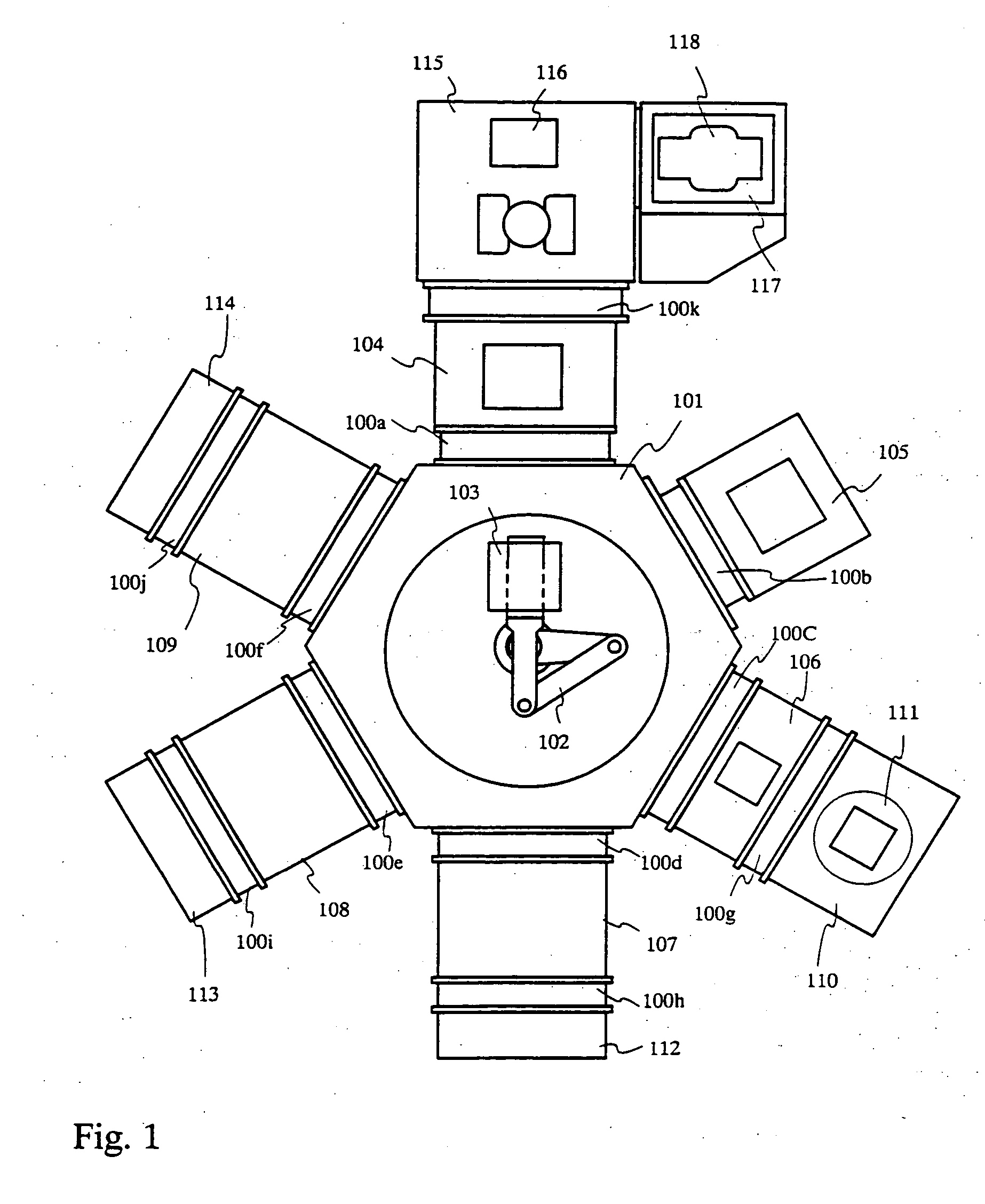
[0055] One example of an organic light emitting element manufacturing device in which the concentration of an impurity such as oxygen or H2O which is contained in an organic compound can be reduced is explained with reference to FIG. 1. FIG. 1 shows a device for conducting the formation of a layer comprised of an organic compound and a cathode and conducting sealing. A conveying chamber 101 is coupled to a load chamber 104, a pre-processing chamber 105, a middle chamber 106, film forming chambers 107 to 109 through gates 100a to 100f, respectively. The pre-processing chamber 105 is provided with the purpose of processing of releasing gas and surface reforming of a substrate to be processed, and a heating process in vacuum and a plasma process using an inert gas are possible in the pre-processing chamber 105.

[0056] The film forming chambers 107 and 108 are processing chambers for forming a film mainly comprised of a low molecular weight organic compound by an evaporation method, and...

embodiment 2

[0073] The organic light emitting element manufactured by using the film forming device in Embodiment 1 is not limited in terms of structure. The organic light emitting element is composed of an anode formed of a conductive film with a light transmitting property, a cathode containing an alkali metal and a layer comprised of an organic compound therebetween. The layer comprised of the organic compound consists of one layer or a plurality of layers. The respective layers are separately referred to as a hole injecting layer, a hole transporting layer, a light emitting layer, an electron transporting layer, an electron injecting layer and the like in accordance with the purpose and function. These layers can be formed of either a low molecular weight organic compound material or a polymer organic compound material or formed by appropriately combining both the materials.

[0074] The organic compound material excellent in a hole transporting property is selected for the hole injecting lay...

embodiment 3

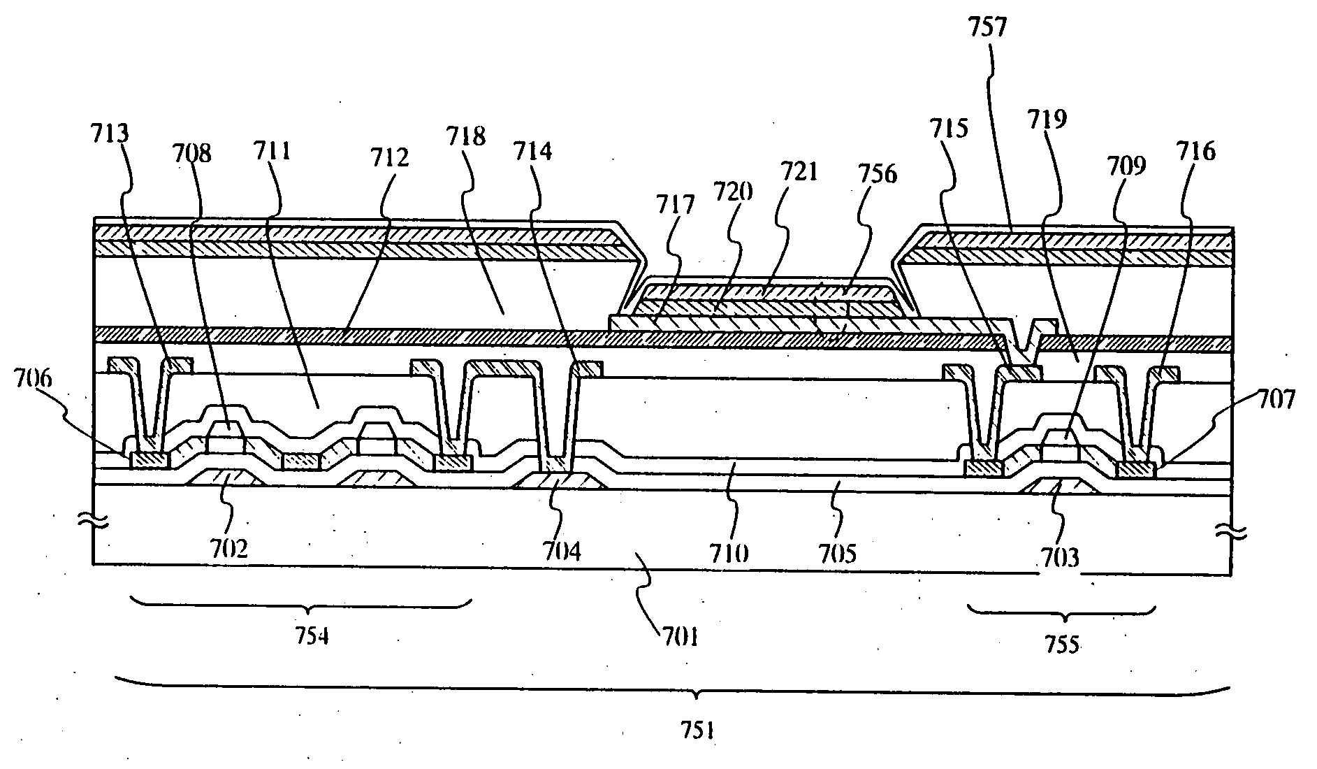
[0083]FIG. 6 shows an example of a structure of an active matrix drive light emitting device. TFTs are provided in a pixel portion and various function circuits in the vicinity thereof. With respect to the TFT, either amorphous silicon or polycrystalline silicon can be selected for the material of a semiconductor film that forms a channel forming region. In the present invention, any of amorphous silicon and polycrystalline silicon may be adopted.

[0084] A glass substrate or an organic resin substrate is adopted for a substrate 601. An organic resin material is lighter than a glass material, and thus, gives a good effect on the reduction in weight of the light emitting device itself. The organic resin materials such as polyimide, polyethylene terephthalate (PET), polyethylene naphthalate (PEN), polyether sulfone (PES) and aramide can be applied in manufacturing the light emitting device. Barium borosilicate glass or alumino borosilicate glass, which is called non-alkali glass, is de...


PUM


Abstract

In an active matrix drive light emitting device, above a thin film transistor, a light emitting element having an anode, a layer comprised of an organic compound and a cathode containing an alkali metal is formed between a third insulating layer comprised of silicon nitride or silicon oxynitride and a fourth insulating layer containing carbon as its main constituent. The light emitting element is formed between partition layers that are formed of an insulating material and have an inverse tapered shape.

Description

BACKGROUND OF THE INVENTION [0001] 1. Field of the Invention [0002] The present invention relates to a phosphor in which luminescence generated by applying electric field (electro luminescence) and to a light emitting device using the phosphor. In particular, the present invention relates to a light emitting device in which an organic compound is used for a phosphor. Fluorescence and phosphorescence are included in the electro luminescence. The present invention relates to a light emitting device to which light emission by one or both of the fluorescence and phosphorescence is applied. [0003] 2. Description of the Related Art [0004] A back light or a front light is used as the typical form of a display device using liquid crystal, and the structure is such that an image is displayed by-means of the light. The liquid crystal display device is adopted as an image displaying means in various electronic devices, but has a defect from the viewpoint of its structure that a viewing angle i...

Claims


Application Information

Patent Timeline
Patent Type & Authority Applications(United States)
IPC IPC(8): H01L27/32H05B33/22
CPCH01L27/3246H01L27/3258H01L27/1248H01L51/5253H01L51/5221H10K59/122H10K59/124H10K50/826H10K50/844H05B33/22
Inventor YAMAZAKI, SHUNPEI
Owner SEMICON ENERGY LAB CO LTD
Why Eureka
Try Eureka