Method of manufacturing amorphous metal oxide film and methods of manufacturing capacitance element having amorphous metal oxide film and semiconductor device

a manufacturing method and technology which are applied in the direction of solid-state devices, coatings, chemical vapor deposition coatings, etc., can solve the problems of insufficient coupling between ta and o, semiconductor devices are required to operate at higher speeds, and the electric characteristics cannot be obtained. , to achieve the effect of improving the film improving the quality of amorphous metal oxide film, and excellent quality

Inactive Publication Date: 2005-05-05
SONY CORP +1
View PDF4 Cites 6 Cited by
  • Summary
  • Abstract
  • Description
  • Claims
  • Application Information

AI Technical Summary

Benefits of technology

[0017] In view of the aforesaid aspects, it is an object of the present invention to provide methods of depositing an amorphous tantalum oxide film, i.e., and amorphous metal oxide film, excellent in quality as a dielectric insulation film by a low-temperature treatment and which can manufacture a capacitance element and a semiconductor device inexpensively.
[0018] In a method of manufacturing an amorphous metal oxide film and a capacitance element, according to an aspect of the present invention, there is provided a method of manufacturing a capacitance element using an amorphous metal oxide film and an amorphous metal oxide film as a capacitance insulation film. This manufacturing method comprises a process for depositing an amorphous metal oxide film and a film quality improvement treatment process for improving the film quality of the amorphous metal oxide film in the state in which an amorphous state of the amorphous metal oxide film is maintained by a high-density plasma radiation treatment based upon ion and radical reactions and which contains at least oxygen at an ion current density higher than 5 mA / cm2.
[0019] According to another aspect of the present invention, there is provided a method of manufacturing a semiconductor device including an amorphous metal oxide film which comprises a process for depositing an amorphous metal oxide film and a film quality improvement treatment process for improving the film quality of the amorphous metal oxide film in the state in which an amorphous state of the amorphous metal oxide film is maintained by a high-density plasma radiation treatment based upon ion and radical reactions and which contains at least oxygen at an ion current density higher than 5 mA / cm2.
[0020] In the methods of manufacturing the capacitance element and the semiconductor device according to the present invention, all treatments, including the treatment for depositing the amorphous metal oxide film, can be carried out at low temperature, to be concrete, at a temperature lower than 430□. As a result, it becomes possible to use a low melting-point metal layer having low resistivity and which is excellent in workability as a low layer electrode, an interconnection layer and the like.
[0021] According to the manufacturing methods of the present invention, since the film-deposition process and the film quality improvement treatment can be carried out within the same reaction chamber, the system can be simplified in arrangement and its workability can be improved.

Problems solved by technology

However, according to this film deposition method, a large amount of carbon (C) and hydroxyl group remains in the deposited film.
Moreover, there is deposited a film which is in short of oxygen so that Ta and O cannot be coupled sufficiently.
As a result, only by this deposited film, there cannot be obtained sufficient electric characteristics, in particular, a leakage current characteristic, a withstand voltage characteristics, a dielectric constant and so forth.
However, in recent years, semiconductor devices have been required to operate at higher speeds.
When the capacitance element having the MIM structure or the like is formed under the above-mentioned circumstances, if a metal oxide film such as a tantalum oxide film is formed as a dielectric insulation layer by the above-mentioned film-deposition method which requires the above-mentioned high-temperature treatment, then problems will arise in the characteristics and reliability of the capacitance element, i.e., the semiconductor device.
However, these metals inevitably encounter poor workability obtained when these metals are formed as microminiaturized patterns.
Moreover, it is unavoidable that these metals require complex manufacturing processes and complex manufacturing facilities, such that the metal layers become expensive.
However, a plasma oxidation treatment executed by a general diode parallel plate plasma treatment system fails to provide sufficiently high film characteristics.
Even when these systems are formed as a single system, it is unavoidable that metal layers should be produced expensively.

Method used


Image

  • Method of manufacturing amorphous metal oxide film and methods of manufacturing capacitance element having amorphous metal oxide film and semiconductor device
  • Method of manufacturing amorphous metal oxide film and methods of manufacturing capacitance element having amorphous metal oxide film and semiconductor device
  • Method of manufacturing amorphous metal oxide film and methods of manufacturing capacitance element having amorphous metal oxide film and semiconductor device

Examples


##ventive example

THIRD INVENTIVE EXAMPLE

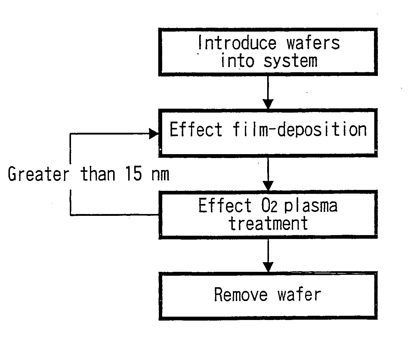
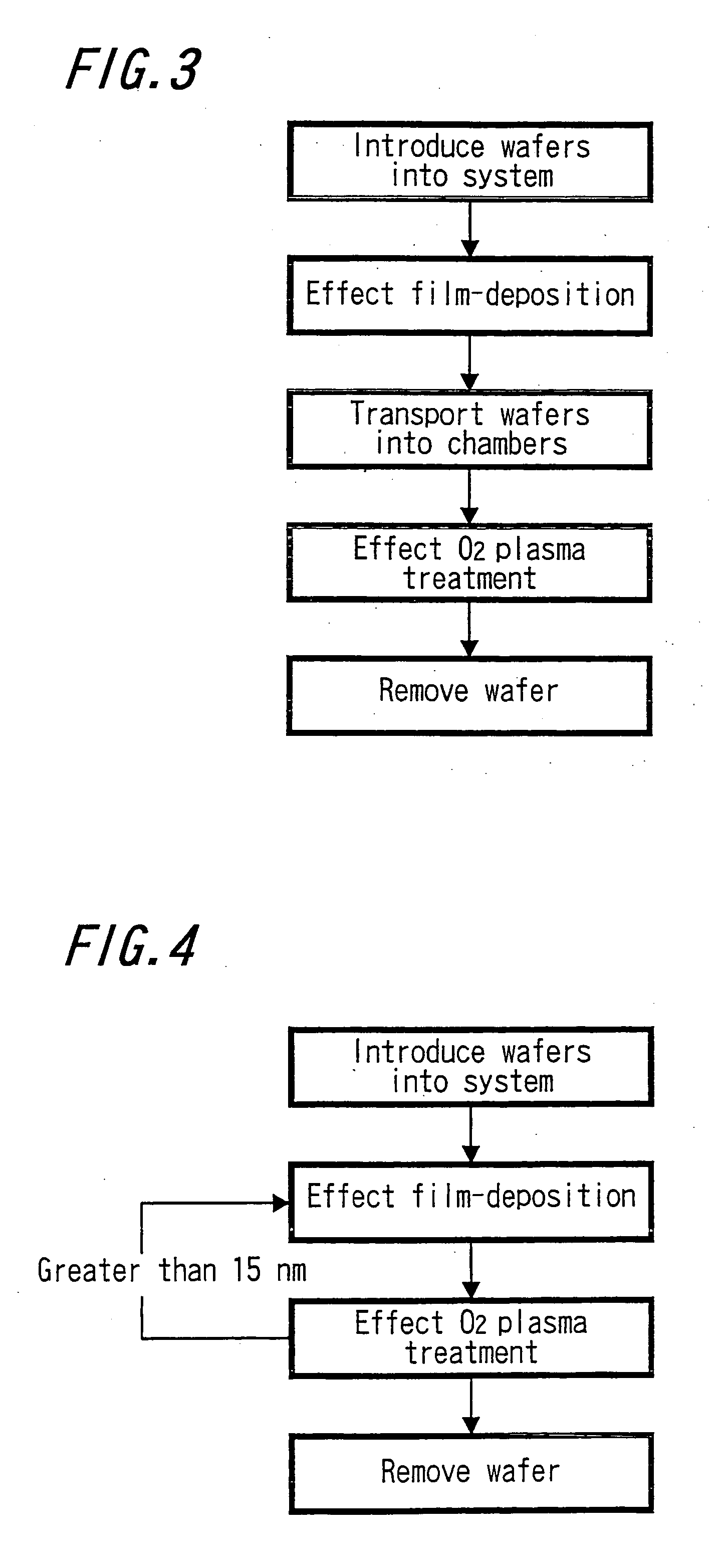
[0068] In this inventive example, as shown in the flowchart of FIG. 5, the film-deposition treatment and the oxidation treatment are continuously carried out within the same reaction chamber.

[0069] This inventive example is a film-deposition process that consists of a film-deposition process using a high-density plasma generation source such as a helicon plasma generation source and a film-quality improvement treatment.

[0070] Specifically, according to the aforementioned diode parallel plate plasma CVD system using the shower head, plasma that can be generated is too low in density to provide a practical film quality and a practical process.

[0071] This will be described below with reference to the flowchart of FIG. 12. In the flowchart shown in FIG. 12, steps identical to those of the flowcharts of FIGS. 4 and 5 are marked by the same reference numerals and therefore need not be described in detail.

[0072] As shown in the flowchart of FIG. 12, the steps req...


PUM

PropertyMeasurementUnit
current densityaaaaaaaaaa
thicknessaaaaaaaaaa
temperatureaaaaaaaaaa

Abstract

A film deposition process for depositing an amorphous metal oxide film, for example, an amorphous tantalum oxide film and a film treatment process for improving film quality of the amorphous tantalum oxide film in the state in which an amorphous state of the amorphous metal oxide film is being maintained by a high-density plasma radiation treatment based upon ion and radical reactions and which contains at least oxygen at an ion current density higher than 5 mA / cm2 are carried out, whereby a low-temperature treatment in the whole process is made possible. In addition, since the amorphous metal oxide film, which is excellent in film quality, can be deposited, the amorphous metal oxide film can be made high in reliability and can be produced inexpensively. The amorphous tantalum oxide film which is excellent in film quality can be manufactured inexpensively by a low-temperature treatment. Also, when a capacitance element having an amorphous metal oxide film and a semiconductor device are manufactured, the amorphous metal oxide film which is excellent in film quality can be deposited by a low-temperature treatment and highly-reliable capacitance element and semiconductor device can be manufactured.

Description

CROSS REFERENCE TO RELATED APPLICATIONS [0001] The present application is a Continuation Application of the patent application Ser. No. 10 / 395,389, filed on Mar. 25, 2003, the entire contents of which are incorporated herein by reference.BACKGROUND OF THE INVENTION [0002] 1. Field of the Invention [0003] The present invention relates to a method of manufacturing amorphous metal oxide films and methods of manufacturing a capacitance element having an amorphous metal oxide film and a semiconductor device having an amorphous metal oxide film, e.g., methods of manufacturing an electrostatic capacitance element using an amorphous metal oxide film formed of an amorphous tantalum oxide thin film as a dielectric insulation film, e.g., a semiconductor device including an amorphous tantalum oxide thin film. [0004] 2. Description of the Related Art [0005] Semiconductor devices, e.g., semiconductor integrated circuit devices, generally use a nitride silicon film (Si3N4 film) as a capacitive ins...

Claims


Application Information

Patent Timeline
Patent Type & Authority Applications(United States)
IPC IPC(8): C23C16/40C23C16/56H01L21/02H01L21/314H01L21/316
CPCC23C16/405H01L28/40H01L21/31604C23C16/56H01L21/02274H01L21/02183H01L21/02323H01L27/04H01L21/0234
Inventor ADACHI, KIWAMUHORIUCHI, SATOSHIYUKIMOTO, TETSUYA
Owner SONY CORP
Why Eureka
Try Eureka