Method of in-situ damage removal - post O2 dry process

a dry process and in-situ technology, applied in the field of integrated circuit fabrication, can solve the problems of degrading device performance, affecting the operation of the instrument, and requiring a large rework process to remove defects,

Inactive Publication Date: 2005-05-19
TAIWAN SEMICON MFG CO LTD
View PDF12 Cites 59 Cited by
  • Summary
  • Abstract
  • Description
  • Claims
  • Application Information

AI Technical Summary

Benefits of technology

[0013] A further objective of the present invention is to provide a dry process for removing oxide residues from a substrate that prevents micro mask defects and does not damage exposed dielectric layers including ILD and IMD layers, and an etch stop layer.
[0014] A still further objective of the present invention is to provide a dry process for removing oxide residues from a substrate that is versatile and may be employed for a variety of applications including the fabrication of STI features, a gate electrode, and an interconnect in a microelectronics device.

Problems solved by technology

Although a conventional buffered HF treatment could be used to remove the oxide residues 8, this method is not recommended since the wet etchant may attack the substrate 1 below pad oxide regions 2 to form grooves (not shown) that degrade device performance.
An expensive rework process is necessary to remove the defects 1a.
Unfortunately, sputtering can easily damage a substrate, especially the top corners of openings in a patterned layer so that critical dimension (CD) control is lost.

Method used


Image

  • Method of in-situ damage removal - post O2 dry process
  • Method of in-situ damage removal - post O2 dry process
  • Method of in-situ damage removal - post O2 dry process

Examples


first embodiment

[0029] Therefore, three embodiments of the present invention are provided although those skilled in the art will appreciate that other applications of the oxide residue removal method of this invention which are not discussed herein are possible. A first embodiment is depicted in FIGS. 1, 2, 4, and 5.

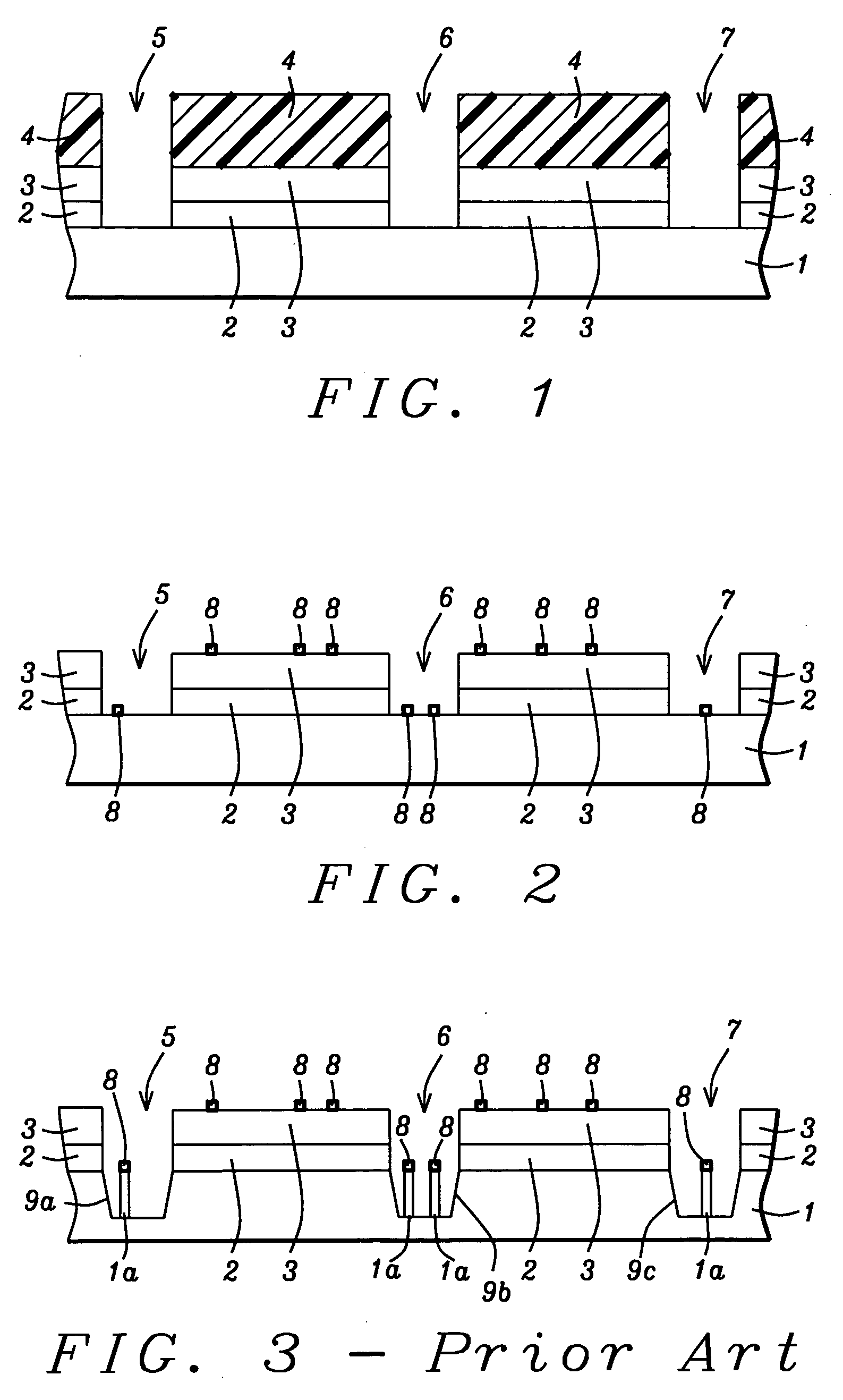
[0030] Although FIGS. 1 and 2 were described previously, a more detailed description is now provided of the various elements therein as they apply to the present invention. Referring to FIG. 1, a substrate 1 is shown that is typically silicon but may optionally be comprised of silicon-on-insulator (SOI), silicon-germanium (SiGe), gallium-arsenide (GaAs) or other semiconductor materials used in the art. The pad oxide layer 2 is grown on substrate 1 by a rapid thermal oxidation (RTO), for example, or may be deposited by a chemical vapor deposition (CVD) method. The pad oxide layer 2 has a thickness between about 30 and 300 Angstroms. A hard mask layer 3 comprised of silicon nitride or pol...

second embodiment

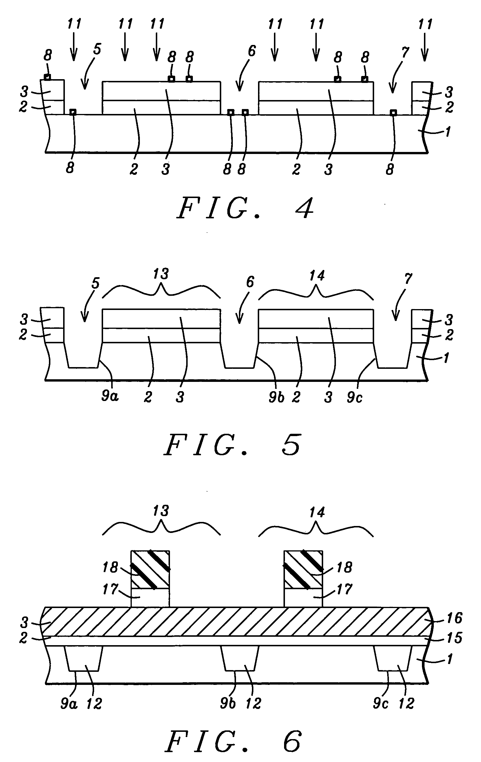
[0039] Referring to FIG. 6, a structure is shown that in an exemplary process flow of the second embodiment is derived from the structure pictured in FIG. 5 in which the active regions 13, 14 are formed between the shallow trenches 9a, 9b and 9b, 9c, respectively. The shallow trenches 9a, 9b, 9c are then filled with an insulating layer 12 such as SiO2 or a low k dielectric layer by a CVD, PECVD, or a spin-on method. Optionally, an oxide liner (not shown) may be grown on the sidewalls and bottom of the shallow trenches 9a, 9b, 9c prior to deposition of the insulating layer 12. Typically, the insulating layer 12 is planarized by a chemical mechanical polish (CMP) process and hard mask 3 and pad oxide 2 are then removed by methods well known to those skilled in the art. For instance, a H3PO4 treatment may be used to remove a silicon nitride hard mask 3 while a dip in a dilute HF solution may be performed to remove a pad oxide layer 2. Although the insulating layer 12 is shown as coplan...

third embodiment

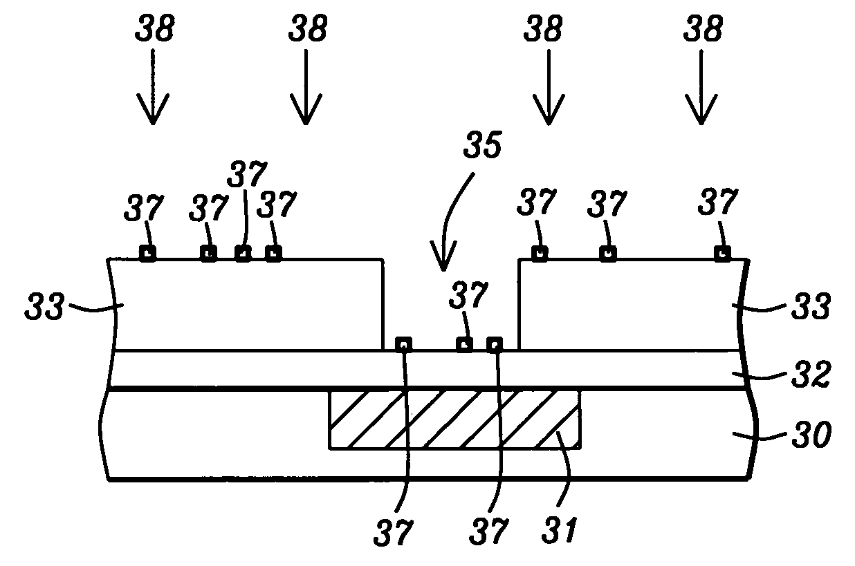
[0047] A third embodiment is depicted in FIGS. 10-13 and involves an integrated process flow in which a first oxygen ashing step is used to remove a photoresist layer over a dielectric layer but generates oxide residues. A plasma step then removes oxide residues and an exposed etch stop layer at the bottom of an opening as part of a damascene scheme to fabricate an interconnect. An additional plasma step removes polymers that are generated by the previous plasma step.

[0048] Referring to FIG. 10, a substrate 30 is shown which is typically silicon but may optionally be comprised of silicon-on-insulator (SOI), silicon-germanium (SiGe), gallium-arsenide (GaAs) or other semiconductor materials used in the art. A conductive layer 31 is formed in substrate 30 by conventional means and has a top surface that is coplanar with the top surface of substrate 30. Optionally, a thin diffusion barrier layer (not shown) is formed along the sides and bottom of the conductive layer 31 to protect the c...


PUM

PropertyMeasurementUnit
temperatureaaaaaaaaaa
pressureaaaaaaaaaa
pressureaaaaaaaaaa

Abstract

An integrated process flow including a plasma step for removing oxide residues following oxygen ashing of a photoresist layer is disclosed. The oxide removal step is effective in preventing micro mask defects and is preferably performed in the same process chamber used for the oxygen ashing step and for a subsequent plasma etch used for pattern transfer. The oxide removal step takes less than 60 seconds and involves a halogen containing plasma that is generated from one or more of NF3, Cl2, CF4, CH2F2, and SF6. Optionally, HBr or a fluorocarbon CXFYHZ where x and y are integers and z is an integer or is equal to 0 may be used alone or with one of the aforementioned halogen containing gases. The oxide removal step may be incorporated in a variety of applications including a damascene scheme, shallow trench (STI) fabrication, or formation of a gate electrode in a transistor.

Description

FIELD OF THE INVENTION [0001] The invention relates to the field of integrated circuit fabrication and in particular to a method of removing oxide residues from a substrate after an oxygen plasma step and before subsequent processing that may include etching an exposed portion of a substrate or removing an underlayer. BACKGROUND OF THE INVENTION [0002] Two of the more important processes that are repeated numerous times during the fabrication of a semiconductor device are photoresist patterning and plasma etching which transfer a pattern from a mask into a photoresist layer and then into one or more underlying layers. The patterned photoresist layer serves as a mask while openings such as vias and trenches in the photoresist layer provide a pathway for reactive ions to remove an exposed underlying layer, or in some cases, more than one underlying layer in an integrated process flow. [0003] A photoresist layer is not thermally stable at temperatures above approximately 150° C. and th...

Claims


Application Information

Patent Timeline
Patent Type & Authority Applications(United States)
IPC IPC(8): G03F7/42H01L21/302H01L21/306H01L21/311H01L21/461H01L21/768
CPCG03F7/427H01L21/02046H01L21/02063H01L21/76814H01L21/31138H01L21/76802H01L21/31116
Inventor CHIU, YUAN-HUNGCHANG, MING-CHINGTAO, HUN-JAN
Owner TAIWAN SEMICON MFG CO LTD
Why Eureka
Try Eureka