Drain extended MOS transistor with improved breakdown robustness

a technology of extended mos and transistors, applied in the field of semiconductor integrated circuit construction, can solve the problems of easy damage, shallow junctions, and difficult integration of many system functions into fewer integrated circuits for certain types of electronic systems

Active Publication Date: 2005-05-26
TEXAS INSTR INC
View PDF14 Cites 68 Cited by
  • Summary
  • Abstract
  • Description
  • Claims
  • Application Information

AI Technical Summary

Benefits of technology

[0018] It is therefore an object of this invention to provide a drain-extended metal-oxide-semiconductor transistor structure that can tolerate reverse breakdown events without being damaged.

Problems solved by technology

However, the integration of many system functions into fewer integrated circuits is difficult for certain types of electronic systems, especially those that must interface with relatively high voltages, such as communications systems.
Conversely, modern high-performance logic and memory circuits operate at decreasing power supply voltages, permitting high density integration of today's complex functionality by way of extremely small transistors, which have structures that cannot tolerate high voltages.
For example, modern high-performance metal-oxide-semiconductor (MOS) transistors have extremely thin gate oxide layers, and also extremely shallow junctions, both of which can be easily damaged by overvoltage.
These colliding trends cause a tradeoff between high-voltage robustness, on one hand, and device density and performance, on the other hand.
The obvious conclusion from these two sweeps SW1 and SW2 is that the DEMOS device was damaged when entering reverse breakdown even a single time.
While the cause of this breakdown damage is not exactly known, it is believed that this breakdown damage is due to the breakdown occurring in a highly localized manner within the device.
Conduction of this parasitic n-p-n transistor can cause further current crowding, which eventually leads to filamentation, and increase in current flow between drain and source.
However, the doping concentration of the wells in regular (i.e., non-drain-extended) MOS devices cannot be increased without adversely affecting the performance of those devices; accordingly, the formation of different well regions for the DEMOS and normal MOS devices requires additional mask and implant steps, and is thus quite costly.
However, this negative backgate bias prevents the sharing of the well of the DEMOS device with normal MOS devices, and also will change the threshold voltage of the transistors which may, in turn, require adjustment of the gate oxide thickness.
However, this integrated source construction of course constrains the DEMOS devices to have a zero volt backgate bias, and prevents the fabrication of symmetric p-channel and n-channel DEMOS transistors in the same integrated circuit.

Method used


Image

  • Drain extended MOS transistor with improved breakdown robustness
  • Drain extended MOS transistor with improved breakdown robustness
  • Drain extended MOS transistor with improved breakdown robustness

Examples


Embodiment Construction

[0031] The present invention will be described in connection with its preferred embodiment, namely as implemented into an n-channel drain-extended metal-oxide-semiconductor (DEMOS, or drain-extended MOS) transistor formed into a bulk silicon substrate. This exemplary embodiment is believed to especially benefit from this invention, as will its complementary p-channel DEMOS devices. However, it is also contemplated that this invention will have benefit in other implementations, including transistors formed into other substrate arrangements such as silicon-on-insulator, depletion mode field-effect transistors (FETs), junction FETs, and the like. Accordingly, it is to be understood that the following description is provided by way of example only, and is not intended to limit the true scope of this invention as claimed.

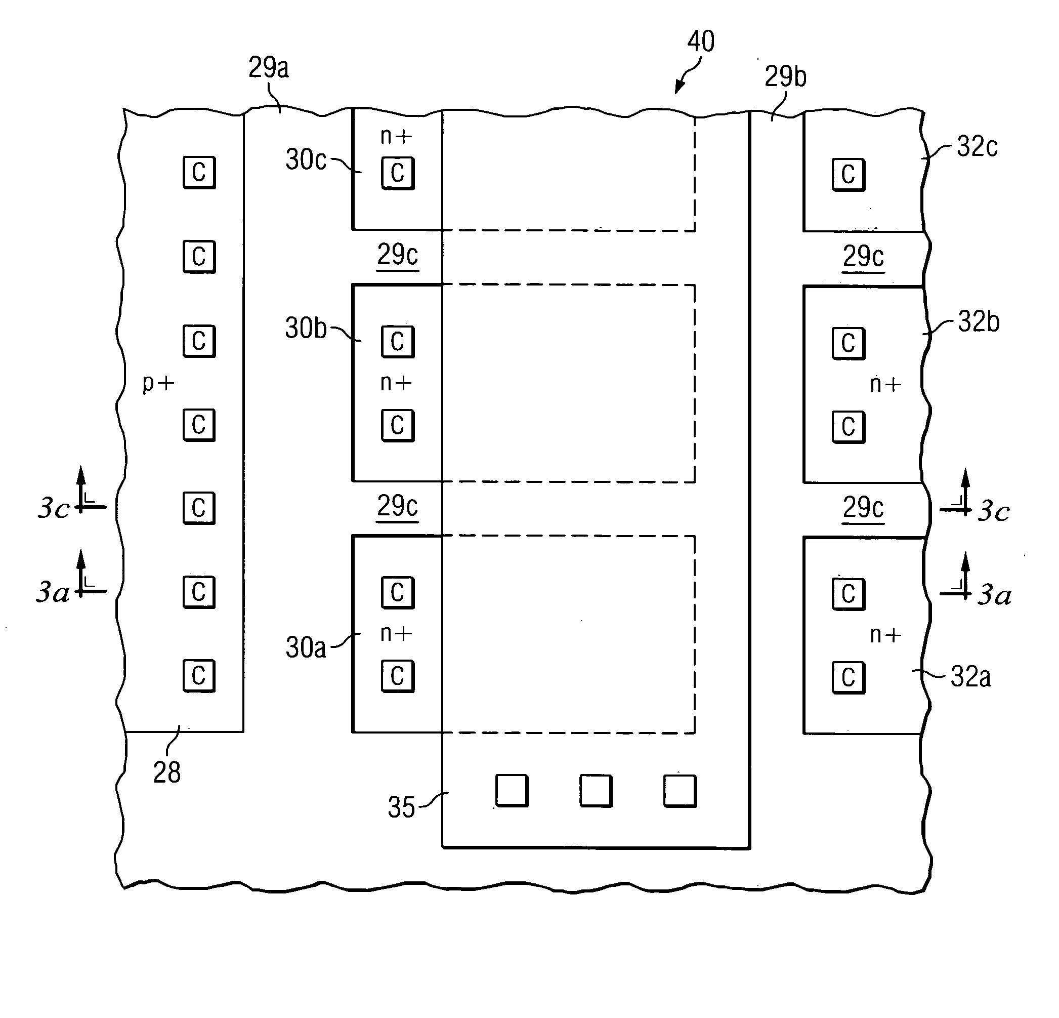
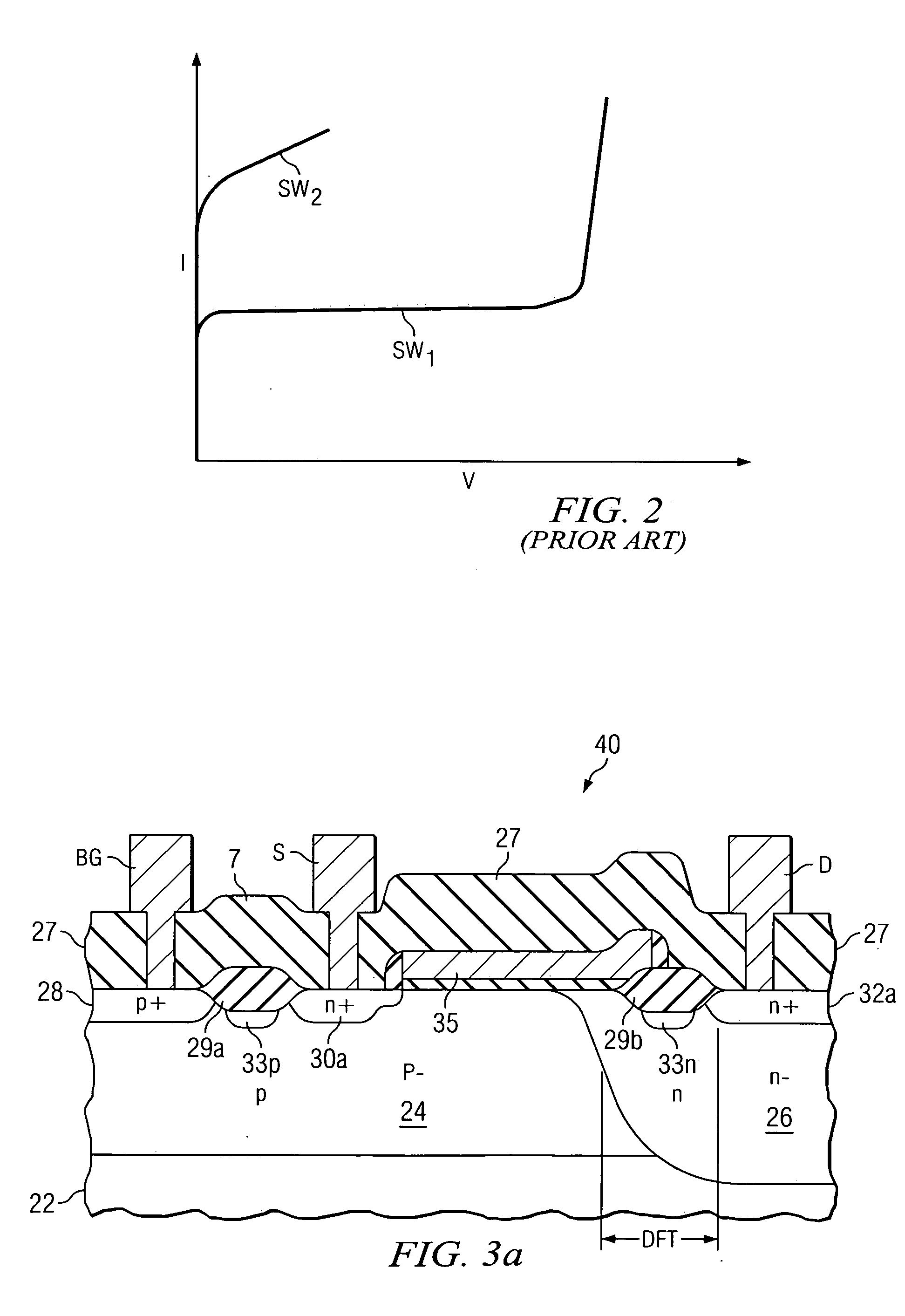
[0032] Referring now to FIGS. 3a through 3c, n-channel drain-extended MOS transistor 40 constructed according to the preferred embodiment of the invention will now be d...


PUM


Abstract

A drain-extended metal-oxide-semiconductor transistor (40) with improved robustness in breakdown characteristics is disclosed. Field oxide isolation structures (29c) are disposed between the source region (30) and drain contact regions (32a, 32b, 32c) to break the channel region of the transistor into parallel sections. The gate electrode (35) extends over the multiple channel regions, and the underlying well (26) and thus the drift region (DFT) of the transistor extends along the full channel width. Channel stop doped regions (33) underlie the field oxide isolation structures (29c), and provide conductive paths for carriers during breakdown. Parasitic bipolar conduction, and damage due to that conduction, is therefore avoided.

Description

CROSS-REFERENCE TO RELATED APPLICATIONS [0001] Not applicable. STATEMENT REGARDING FEDERALLY SPONSORED RESEARCH OR DEVELOPMENT [0002] Not applicable. BACKGROUND OF THE INVENTION [0003] This invention is in the field of semiconductor integrated circuits, and is more specifically directed to the construction of transistors in such circuits. [0004] A continuing trend in the field of electronic devices and systems is the integration of system functions into fewer integrated circuits. Larger-scale integration provides improved device and system performance, because of such factors as the excellent matching among transistors within the same integrated circuit, the very short conduction path lengths among functions on the same integrated circuit, and the elimination of interface circuitry that is necessary for communication of signals between separate integrated circuits. These benefits are attained along with the significantly lower manufacturing cost with these fewer integrated circuits ...

Claims


Application Information

Patent Timeline
Patent Type & Authority Applications(United States)
IPC IPC(8): H01L29/06H01L29/423H01L29/76H01L29/78H01L29/94H01L31/062H01L31/113H01L31/119
CPCH01L29/0615H01L29/0638H01L29/7835H01L29/0692H01L29/42368H01L29/0653
Inventor PENDHARKAR, SAMEER P.
Owner TEXAS INSTR INC
Why Eureka
Try Eureka