Silicon-based Schottky barrier infrared optical detector

a technology of infrared optical detectors and silicon-based schottky barriers, which is applied in the direction of optical elements, optical waveguide light guides, instruments, etc., can solve the problems of large scattering loss along the sidewalls of the rib waveguide structure, low external quantum efficiency levels, and large loss of scattering loss, etc., to achieve low dark current and operate efficiently at room temperature

Active Publication Date: 2005-05-26
CISCO TECH INC
View PDF3 Cites 81 Cited by
  • Summary
  • Abstract
  • Description
  • Claims
  • Application Information

AI Technical Summary

Benefits of technology

[0006] The need remaining in the prior art is addressed by the present invention, which relates to a silicon-based Schottky barrier infrared (IR) optical det...

Problems solved by technology

Incident light is applied perpendicular to (i.e., “normal to”) this structure, passing through the relatively thin metallic film, where the thin film absorbs only a portion of the light, thus resulting in extremely low external quantum efficiency levels.
However, as the detection area increases, the dark current (unwanted noise signal) increases as well.
Moreover, while relatively simple in structure, such normal incidence detectors typically require cooling, again associated with a relatively high dark current value.
While an improvement in absorption efficiency may be achieved with the Yang et al. structure, significant losses remain in terms of scattering losses along the si...

Method used


Image

  • Silicon-based Schottky barrier infrared optical detector
  • Silicon-based Schottky barrier infrared optical detector
  • Silicon-based Schottky barrier infrared optical detector

Examples


Embodiment Construction

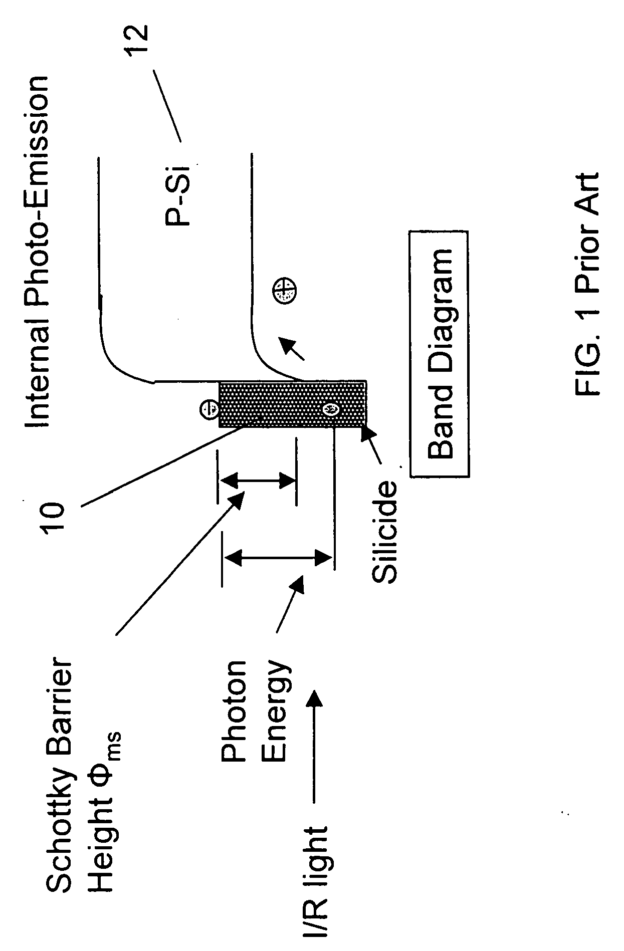
[0031] As described above, the present invention is directed to a monolithically integrated, planar Schottky barrier infrared waveguide detector capable of operating below, at or above room temperature. Advantageously, the fabrication process and materials of the inventive detector are compatible with conventional, planar CMOS process technology associated with the semiconductor industry.

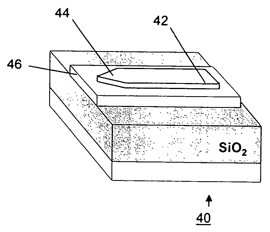
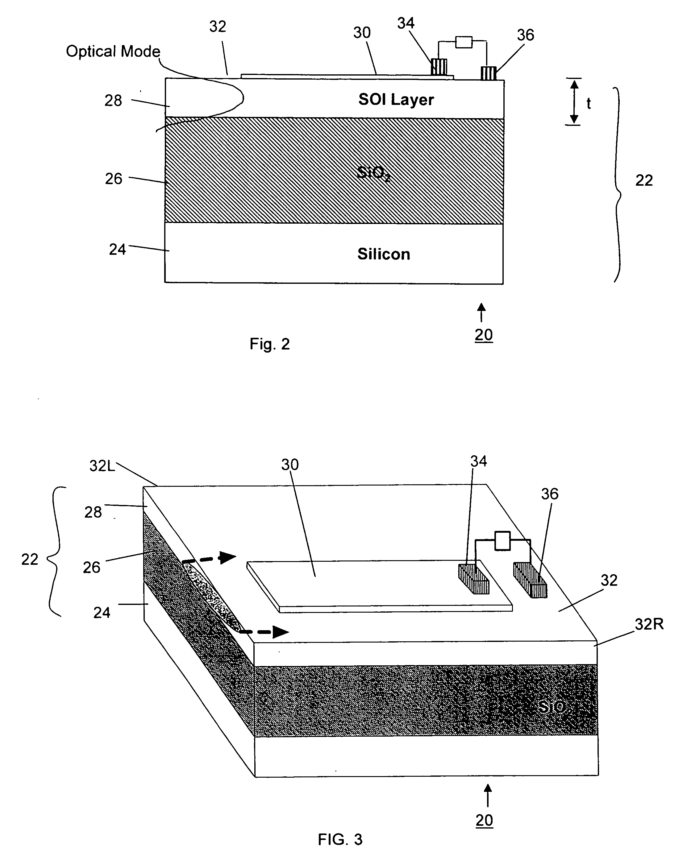
[0032] In accordance with the present invention, a Schottky barrier junction is formed on the sub-micron thick, planar silicon waveguiding surface layer (“SOI layer”) of an SOI structure. This Schottky barrier junction is formed in such a way that the optical signal propagating laterally along a waveguide within the planar SOI layer (traveling in the direction parallel to the junction) is continuously absorbed into the overlying silicide layer as it passes thereunder. As a result of this geometry, even a relatively thin silicide layer (e.g., a few monolayers thick) will absorb a large portion of th...


PUM


Abstract

A silicon-based IR photodetector is formed within a silicon-on-insulator (SOI) structure by placing a metallic strip (preferably, a silicide) over a portion of an optical waveguide formed within a planar silicon surface layer (i.e., “planar SOI layer”) of the SOI structure, the planar SOI layer comprising a thickness of less than one micron. Room temperature operation of the photodetector is accomplished as a result of the relatively low dark current associated with the SOI-based structure and the ability to use a relatively small surface area silicide strip to collect the photocurrent. The planar SOI layer may be doped, and the geometry of the silicide strip may be modified, as desired, to achieve improved results over prior art silicon-based photodetectors.

Description

CROSS-REFERENCE TO RELATED APPLICATION [0001] This application claims the benefit of Provisional Application No. 60 / 523,846, filed Nov. 20, 2003.TECHNICAL FIELD [0002] The present invention relates to a silicon-based Schottky barrier infrared (IR) optical detector and, more particularly, to a planar, waveguide-based IR optical detector with sufficiently low dark current to operate efficiently at room temperature. BACKGROUND OF THE INVENTION [0003] Semiconductor devices using metal-semiconductor barriers (referred to as Schottky barriers) instead of p-n junctions have been developed to convert incident light into electrical energy. Silicon is often used as the semiconductor material in Schottky barrier photodetectors operating in the IR portion of the electromagnetic energy spectrum. In its most conventional form, a silicon-based Schottky barrier photodiode consists of a thin metallic film (such as a silicide film) disposed on a silicon layer. Incident light is applied perpendicular ...

Claims


Application Information

Patent Timeline
IPC IPC(8): G02B6/12G02B6/122H01L31/00H01L31/0224H01L31/0232H01L31/0392H01L31/108H01L31/153
CPCG02B6/12004G02B6/1228H01L31/022408Y02E10/50H01L31/03921H01L31/108H01L31/153H01L31/0232G02B6/12G02B6/122H01L31/0224
Inventor PATEL, VIPULKUMARGHIRON, MARGARETGOTHOSKAR, PRAKASHMONTGOMERY, ROBERT KEITHPATHAK, SOHAMPIEDE, DAVIDSHASTRI, KALPENDUYANUSHEFSKI, KATHERINE A.
Owner CISCO TECH INC
Why Eureka
Try Eureka