Method for manufacturing semiconductor device

a manufacturing method and semiconductor technology, applied in the field of semiconductor devices, can solve the problems of difficult to reduce the highest temperature of a process, difficult to make glass substrates and quartz substrates larger, and easy cracking and heavy, and achieve the effect of preferable yield

Inactive Publication Date: 2005-05-26
SEMICON ENERGY LAB CO LTD
View PDF41 Cites 42 Cited by
  • Summary
  • Abstract
  • Description
  • Claims
  • Application Information

AI Technical Summary

Benefits of technology

[0011] It is an object of the present invention to provide a method for peeling without damaging a peeling layer, and to pee

Problems solved by technology

Although a glass substrate and a quartz substrate are widely utilized at present, there is a disadvantage of being easily cracked and heavy.
Moreover, a glass substrate and a quartz substrate are difficult to be made larger on the basis of mass-production, and these are not suitable for that.
However, since the heat resistance of a plastic film is low, it cannot help lowering the highest temperature of a process.
As a result, a TFT which has not so excellent electric characteristics compared with those formed over a glass substrates is formed at present.
Therefore, a liquid crystal display device and a light emitting element having a high perfor

Method used


Image

  • Method for manufacturing semiconductor device
  • Method for manufacturing semiconductor device
  • Method for manufacturing semiconductor device

Examples


embodiment mode 1

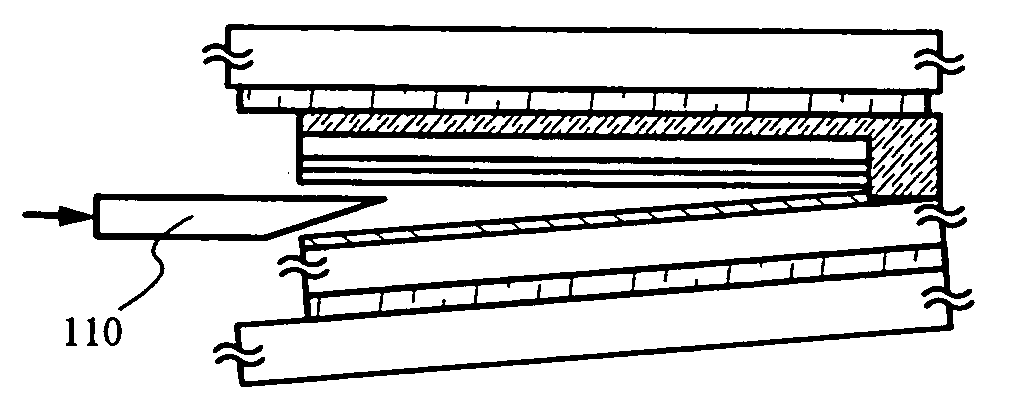
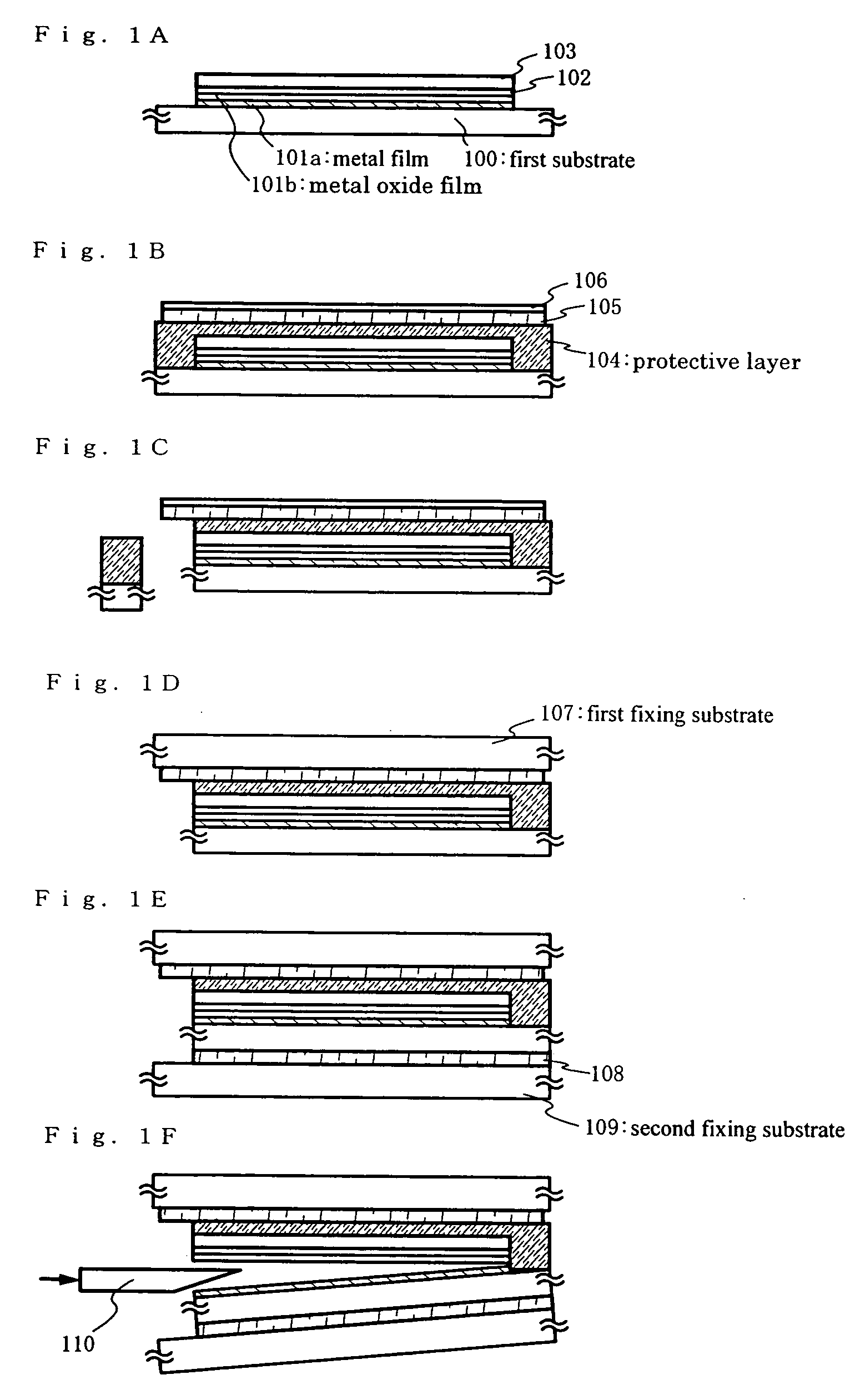
[0056] Here, a method for peeling with the use of a metal film and a silicon oxide film is used.

[0057] Initially, a peeling layer 103 which includes a semiconductor integrated circuit (here, a CPU), a terminal electrode (not shown), and an alignment marker (not shown) is formed over a first substrate 100.

[0058] A metal film 101a, here, a tungsten film (a film thickness of from 10 nm to 200 nm, preferably from 30 nm to 75 nm) is formed by sputtering, and an oxide film 102, here, a silicon oxide film (a film thickness of from 150 nm to 200 nm) is further laminated over the substrate without being exposed to the atmospheric air by sputtering. The film thickness of the oxide film 102 is desirably twice that of the metal film. At the time of laminating, a metal oxide film (a tungsten oxide film) in an amorphous state is formed with a thickness of from 2 nm to 5 nm between the metal film 101a and the silicon oxide film 102. In peeling in a later step, separation occurs inside the tungst...

embodiment mode 2

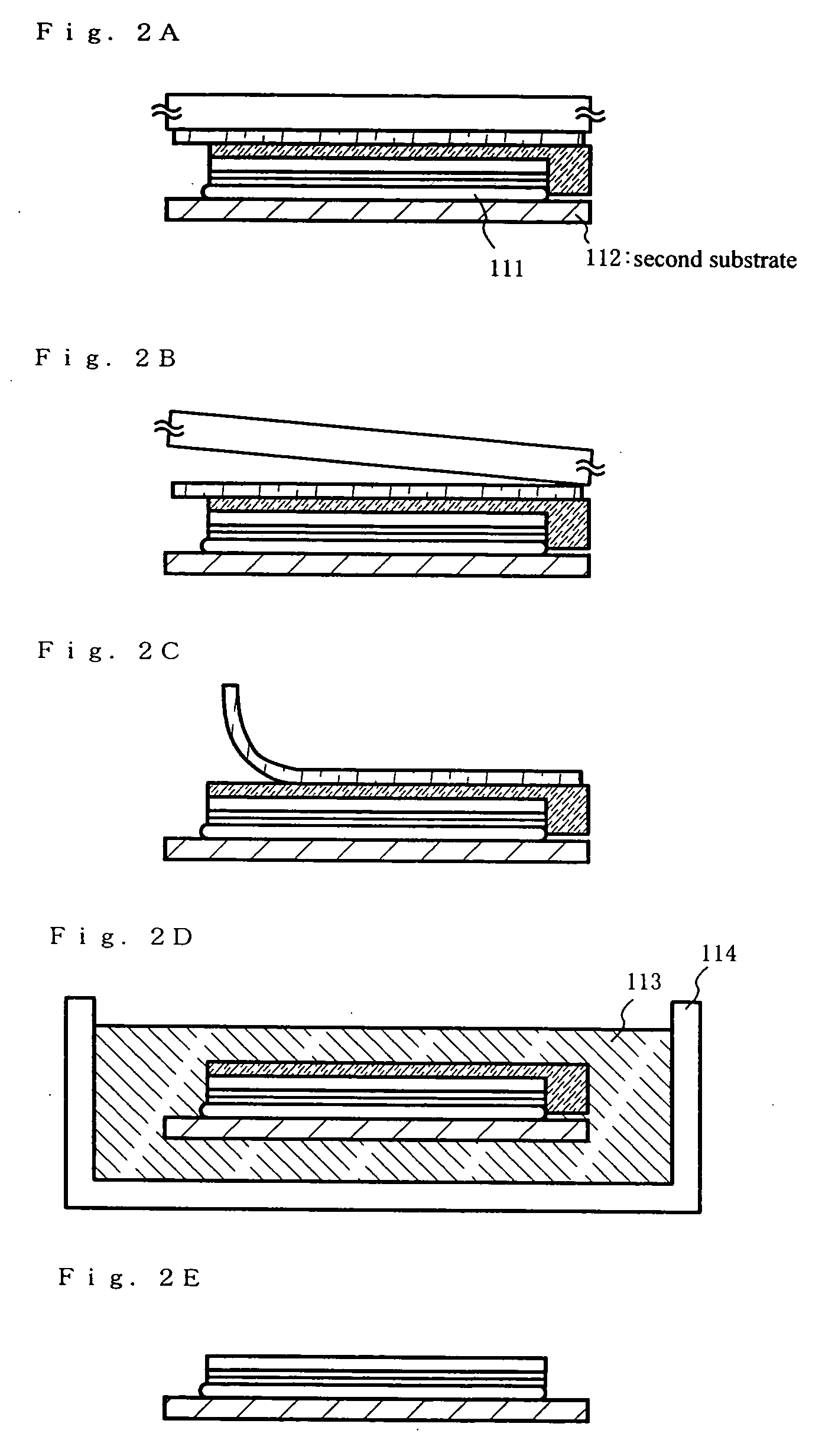
[0092] Here, when an FPC is pressure-bonded to a device which is transferred to a flexible substrate such as a plastic film, a method for preventing a defect such as a crack and the like is shown with reference to FIGS. 4A to 4C.

[0093] Initially, a peeling layer formed over a glass substrate is transferred to a flexible substrate according to Embodiment Mode 1. After forming a metal film over the glass substrate, at the time of forming an oxide film 404, a metal oxide film in an amorphous state is formed between the metal film and the oxide film. The peeling layer is then formed over the oxide film 404.

[0094] As the peeling layer to be transferred, a layer 405a including a circuit having an element 405a, and a terminal electrode 405b are formed, and a protective layer 405c formed from a resin to prevent a crack is formed thereover.

[0095] The metal oxide film becomes a crystallized metal oxide film 403 by performing heat treatment of 400° C. or more in a process to form the peelin...

embodiment 1

[0102] In this embodiment, an example of transferring a semiconductor integrated circuit, typically, a CPU to a plastic substrate is shown. FIG. 5A shows a cross-sectional view before transferring, and FIG. 5B shows a cross-sectional view after transferring.

[0103] Initially, a metal layer 21 is formed over a thermostability substrate 20 such as a quartz substrate or a glass substrate. In this embodiment, Corning 1737 (or EAGLE 2000) of 5 inches manufactured by Corning Incorporated is used as a glass substrate.

[0104] As a material forming the metal layer 21, an element of tungsten (W), molybdenum (Mo), technetium (Tc), rhenium (Re), ruthenium (Ru), osmium (Os), rhodium (Rh), iridium (Ir), palladium (Pd), and silver (Ag), an alloy containing the element as its main component, or a monolayer or lamination layer of nitride (for example, titanium nitride, tungsten nitride, tantalum nitride, or molybdenum nitride) can be used.

[0105] In this embodiment, the metal film 21, here, a tungst...


PUM


Abstract

It is an object of the invention to provide a peeling method which does not damage a peeling layer, and to perform peeling not only a peeling layer having a small-size area but also an entire peeling layer having a large-size area with a preferable yield. In the invention, after pasting a fixing substrate, a part of a glass substrate is removed by scribing or performing laser irradiation on the glass substrate which leads to providing a trigger. Then, peeling is performed with a preferable yield by performing peeling from the removed part. In addition, a crack is prevented by covering the entire face except for a connection portion of a terminal electrode (including a periphery region of the terminal electrode) with a resin.

Description

BACKGROUND OF THE INVENTION [0001] 1. Field of the Invention [0002] The present invention relates to a semiconductor device having a circuit including a thin film transistor (hereinafter referred to as a TFT), and to a method for manufacturing the same. For example, the invention relates to an electronic device on which an electro-optical device typified by a liquid crystal display panel or a light emitting display device having an organic light emitting element is mounted as its component. [0003] In this specification, the term “semiconductor device” refers to a device in general that utilizes semiconductor characteristics to function, and electro-optical devices, semiconductor circuits and electronic devices are all included in the semiconductor device. [0004] 2. Description of the Related Art [0005] In recent years, a technique for forming a thin film transistor (a TFT) by using a semiconductor thin film (thickness is approximately from several nm to several hundreds nm) formed o...

Claims


Application Information

Patent Timeline
IPC IPC(8): H01L29/786H01L21/762H01L21/77H01L21/84H01L27/12H01L27/32H01L51/52H01L51/56
CPCG02F2001/13613H01L27/1214H01L27/1266H01L27/3244Y10S438/976H01L51/56H01L2221/68368Y10S438/977H01L51/5237G02F1/13613H10K59/122H10K50/841H10K50/8426H10K71/80H10K59/1201H10K50/844H10K71/00H10K59/12H10K50/84H01L27/12
Inventor GOTO, YUUGOFUKUMOTO, YUMIKOTAKAYAMA, TORUMARUYAMA, JUNYATSURUME, TAKUYA
Owner SEMICON ENERGY LAB CO LTD
Why Eureka
Try Eureka