Flip-chip light emitting diode and method of manufacturing the same

a light emitting diode and flip-chip technology, applied in the direction of semiconductor devices, basic electric elements, electrical equipment, etc., can solve the problems of high operating voltage of flip-chip light emitting devices of ito/ag electrode structures, increase of contact resistivity and reflection rate, and rapid increase of contact resistance of top emitting light emitting devices. , to achieve the effect of low contact resistance and high reflection ra

Inactive Publication Date: 2005-06-09
SAMSUNG ELECTRONICS CO LTD +1
View PDF13 Cites 31 Cited by
  • Summary
  • Abstract
  • Description
  • Claims
  • Application Information

AI Technical Summary

Benefits of technology

[0010] The present invention provides a flip-chip type light emitting device having an electrode structure of providing low contact resistivity and a high reflection rate and a method of manufacturing the same.

Problems solved by technology

In other words, a top emitting type light emitting device cannot be used as a light emitting device having a large capacity and high luminance.
However, in such a flip-chip type light emitting device, adherence between the p-type cladding layer and the silver layer is weak, thus a large portion of the silver layer is oxidized or a large number of voids are formed in the silver layer after annealing, resulting in the increase of contact resistivity and the decrease of a reflection rate.
However, the operation voltage of the flip-chip light emitting device of ITO / Ag electrode structure rapidly increases due to the resistivity of ITO, which is higher than the resistivity of nickel / gold by more than three times.

Method used


Image

  • Flip-chip light emitting diode and method of manufacturing the same
  • Flip-chip light emitting diode and method of manufacturing the same
  • Flip-chip light emitting diode and method of manufacturing the same

Examples


first embodiment

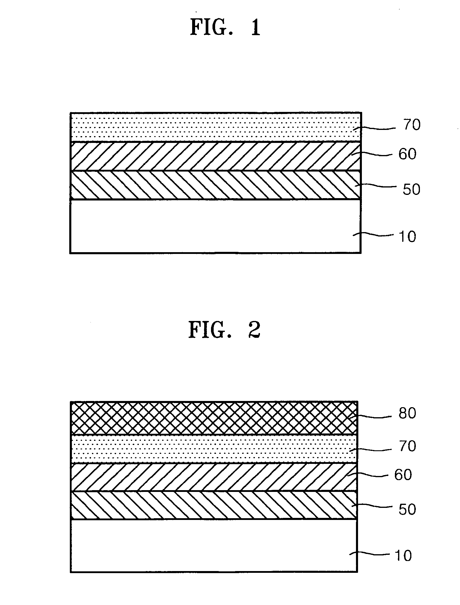
[0038]FIG. 1 is a sectional view of a p-type electrode structure according to the present invention.

[0039] Referring to FIG. 1, a p-type electrode structure includes an ohmic contact layer 60 and a reflection layer 70.

[0040] In the p-type electrode structure of FIG. 1, a nitride based group III cladding layer 50 is formed on a substrate 10, and the ohmic contact layer 60 and the reflection layer 70 are sequentially deposited on the p-type cladding layer 50.

[0041] The p-type cladding layer 50 is formed of a group III nitride compound to which a p-type dopant is doped.

[0042] The group III nitride compound denotes a compound represented by AlxInyGazN (0≦×≦1, 0≦y≦1, 0z≦1, 0≦x+y+z≦1).

[0043] In addition, examples of the p-type dopant include Mg, Zn, Ca, Xr, and Ba.

[0044] The ohmic contact layer 60 is formed of tin oxide to which an addition element is doped.

[0045] An example of the addition element doped to the ohmic contact layer 60 is at least one of antimony (Sb), fluorine (F), p...

second embodiment

[0055]FIG. 2 is a sectional view of a p-type electrode structure according to the present invention.

[0056] In the description of a p-type electrode according to the second embodiment of the present invention of FIG. 2, the elements having the same functions as FIG. 1 are referred to the same reference numerals as FIG. 2.

[0057] Referring to FIG. 2, a p-type electrode structure according to the second embodiment of the present invention includes an ohmic contact layer 60, a reflection layer 70, and a diffusion barrier layer 80.

[0058] In the p-type electrode structure of FIG. 2, a nitride based group III cladding layer 50 is formed on a substrate 10, and the ohmic contact layer 60, the reflection layer 70, and the diffusion barrier layer 80 are sequentially deposited on the p-type cladding layer 50.

[0059] The ohmic contact layer 60 is formed by doping at least one of antimony, fluorine, phosphorus, and arsenic to tin oxide.

[0060] The reflection layer 70 is formed of silver or rhodi...


PUM


Abstract

Provided are a flip-chip type light emitting device and a method of manufacturing the same. The provided flip-chip type light emitting device includes a substrate, an n-type cladding layer, an active layer, a p-type cladding layer, an ohmic contact layer formed of tin oxide to which at least one of antimony, fluorine, phosphorus, and arsenic is doped, and a reflection material formed of a reflective material. According to the provided flip-chip type light emitting device and the method of manufacturing the same, a current-voltage characteristic and durability are improved by applying a conductive oxide electrode structure having low surface resistivity and high carrier concentration.

Description

BACKGROUND OF THE INVENTION [0001] This application claims the priority of Korean Patent Application No. 2003-85600, filed on Nov. 28, 2003, in the Korean Intellectual Property Office, the disclosure of which is incorporated herein in its entirety by reference. [0002] 1. Field of the Invention [0003] The present invention relates to a flip-chip type light emitting device and a method of manufacturing the same, and more particularly, to a flip-chip type light emitting device for improving luminescence efficiency and a method of manufacturing the same. [0004] 2. Description of the Related Art [0005] Conventional gallium nitride based light emitting devices are divided into top emitting type light emitting devices and flip-chip type light emitting devices. A top emitting type light emitting device emits light through an ohmic contact layer, which contacts a p-type cladding layer. In such a top emitting type light emitting device, an electrode structure is formed by sequentially deposit...

Claims


Application Information

Patent Timeline
Patent Type & Authority Applications(United States)
IPC IPC(8): H01L33/06H01L33/10H01L33/32H01L33/34H01L33/42
CPCH01L33/46H01L33/42
Inventor SEONG, TAE-YEONSONG, JUNE-OLEEM, DONG-SEOKHONG, HYUN-GI
Owner SAMSUNG ELECTRONICS CO LTD
Why Eureka
Try Eureka