

Organic element for electroluminescent devices
a technology of electroluminescent devices and organic elements, which is applied in the direction of discharge tube luminescnet screens, other domestic articles, natural mineral layered products, etc., can solve the problems of large efficiency loss, performance limitations, and many desirable applications, and achieve the effect of using phosphorescent light emissions
- Summary
- Abstract
- Description
- Claims
- Application Information
AI Technical Summary
Benefits of technology
Problems solved by technology
Method used
Image

Examples
synthetic example 1
Preparation of Inv-1
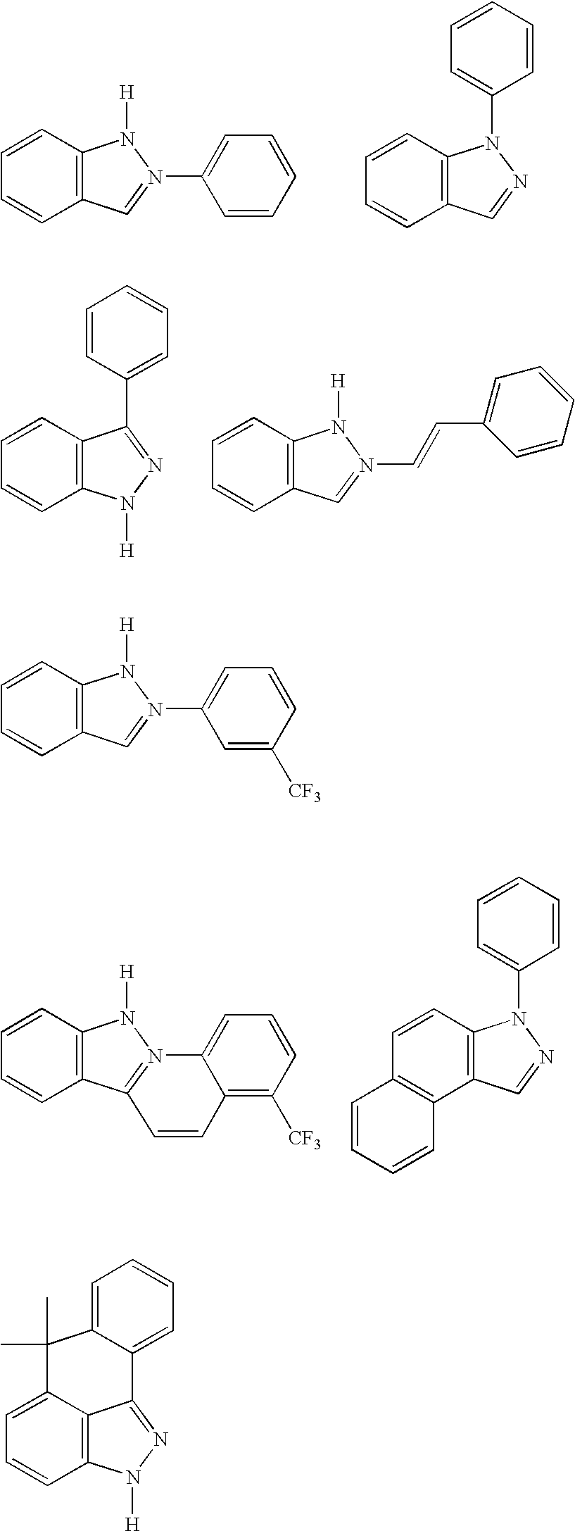
[0163] The ligand, 1-phenylindazole, was prepared by combining indazole (Aldrich, 7.83 g, 66 mmol), iodobenzene (7.0 ml, 63 mmol), copper(I) iodide (0.36 g, 1.9 mmol), 1,2-diaminocyclohexane (0.58 ml, 3.8 mmol), potassium phosphate (24.0 g, 120 mmol) and dioxane (70 mol) under nitrogen, in a 250 ml round bottom flask. The reaction mixture was stirred at reflux for 14 h, allowed to cool to room temperature and the solid materials were separated by filtration. The filtrate was concentrated under reduced pressure; the residue was dissolved in ethyl acetate and washed sequentially with 3% ammonium hydroxide and water. The organic layer was dried with sodium sulfate prior to evaporation. The remaining residue was purified on silica gel using a mixture of heptane and ethyl acetate (5:1) to yield 9.12 g (71%) of 1-phenylindazole.
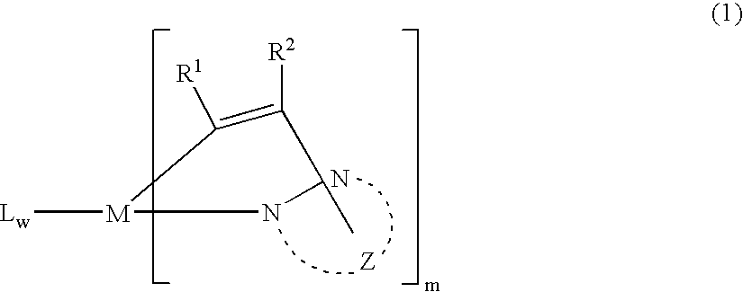
[0164] K3IrBr6 (4.10 g) and 1-phenylindazole (2.52 g) were placed in a 200 mL flask with 48 mL 2-ethoxyethanol and 12 mL water. The mixture w...
synthetic example 2
Preparation of Inv-21
[0166] K3IrBr6 (3.72 g) and 1-(4-fluoro-phenyl)indazole (2.50 g) were placed in a 100 mL flask with 30 mL 2-ethoxyethanol and 10 mL water. The mixture was freeze-thaw degassed and then refluxed under nitrogen for 4 h. After cooling, a yellow precipitate was filtered in air and washed with 1 M HBr (aq) and with water, and dried. Tetrakis(1-(4-fluoro-phenyl)-1H-indazole-N,C)(μ-dibromo)diiridium(III) (3.00 g) was collected and used without further purification in the next reaction.
[0167] Tetrakis(1-(4-fluoro-phenyl)indazole-N,C)(μ-dibromo)diiridium(III) (0.79 g) and 1-(4-fluoro-phenyl)indazole (0.49 g) and silver triflouroacetate (0.38 g) were placed in a 100 mL flask with 35 mL 1,2-propanediol. The mixture was freeze-thaw degassed and then refluxed under nitrogen for 4 h. After cooling, an olive precipitate was filtered in air and washed with methanol and dried (1.02 g). A portion of this crude product (0.65 g) was dissolved in methylene chloride and filtered to...
example 1
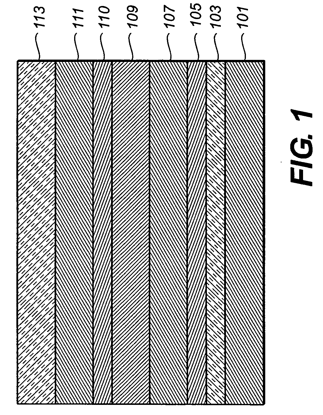
DEVICE EXAMPLE 1
[0168] An EL device (Sample 1) satisfying the requirements of the invention was constructed in the following manner: [0169] 1. A glass substrate coated with an 85 nm layer of indium-tin oxide (ITO) as the anode was sequentially ultrasonicated in a commercial detergent, rinsed in deionized water, degreased in toluene vapor and exposed to oxygen plasma for about 1 min. [0170] 2. Over the ITO was deposited a 1 nm fluorocarbon (CFx) hole-injecting layer (HIL) by plasma-assisted deposition of CHF3. [0171] 3. A hole-transporting layer (HTL) of N,N′-di-1-naphthyl-N,N′-diphenyl-4,4′-diaminobiphenyl (NPB) having a thickness of 75 nm was then evaporated from a tantalum boat. [0172] 4. A 35 nm light-emitting layer (LEL) of 4,4′-N,N′-dicarbazole-biphenyl (CBP) and Inv-1 (4% wt %) were then deposited onto the hole-transporting layer. These materials were also evaporated from tantalum boats. [0173] 5. A hole-blocking layer of bis(2-methyl-quinolinolate)(4-phenylphenolate) (Al(Balq...
PUM
| Property | Measurement | Unit |
|---|---|---|
| wt % | aaaaa | aaaaa |
| thick | aaaaa | aaaaa |
| thickness | aaaaa | aaaaa |
Abstract
Description
Claims
Application Information