Gallium nitride material structures including isolation regions and methods

Inactive Publication Date: 2005-07-07
NITRONEX
View PDF75 Cites 91 Cited by
  • Summary
  • Abstract
  • Description
  • Claims
  • Application Information

AI Technical Summary

Benefits of technology

[0009] In another embodiment, a method is provided. The method comprises forming an isolation region in a gallium nitride material region of a FET; and forming a

Problems solved by technology

Despite the attractive properties noted above, a number of challenges exist when developing gallium nitride material-based devices.
For example, leakage current can sacrifice performance in gallium nitride material-based devices (e.g., transistors).

Method used


Image

  • Gallium nitride material structures including isolation regions and methods
  • Gallium nitride material structures including isolation regions and methods
  • Gallium nitride material structures including isolation regions and methods

Examples


example 1

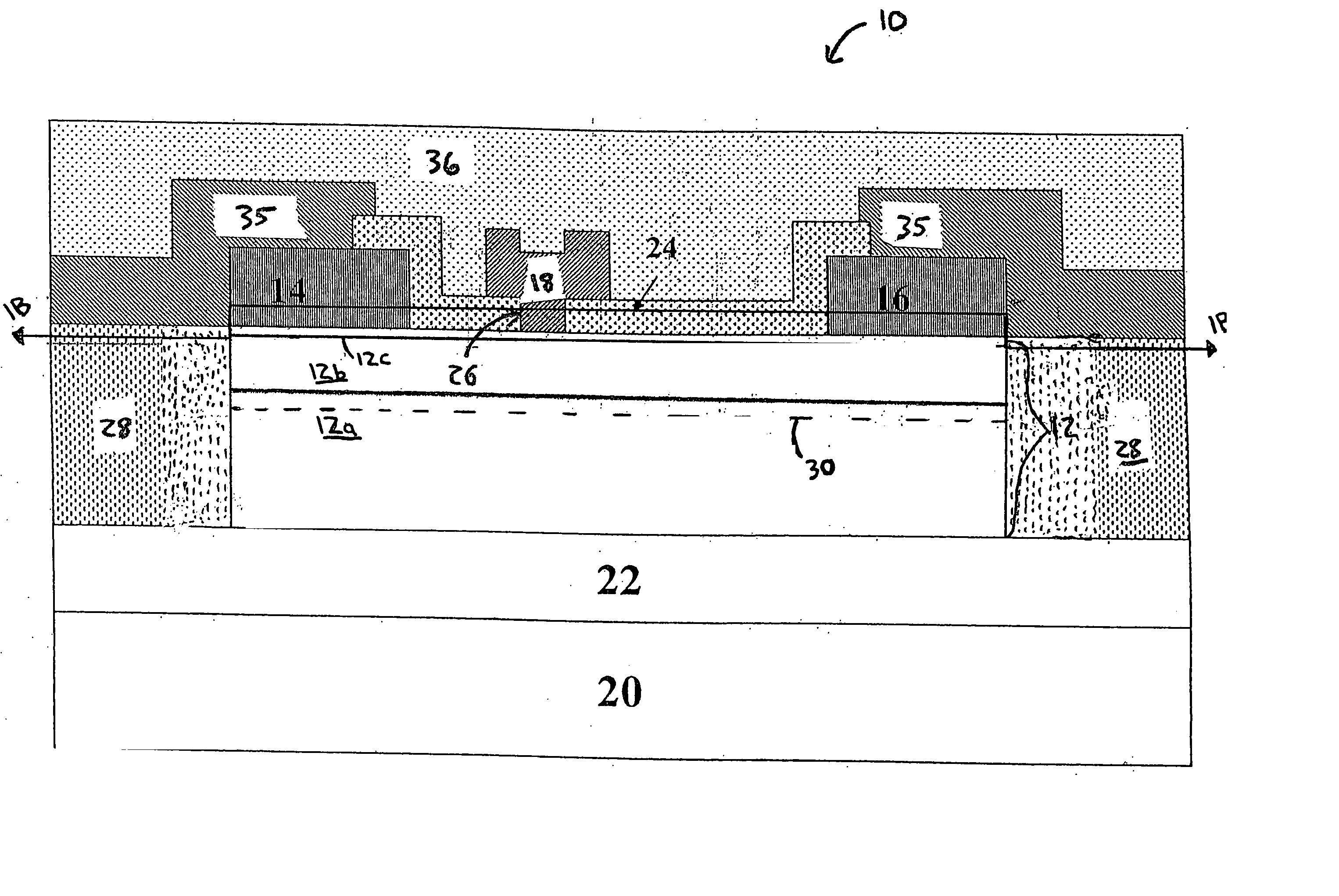
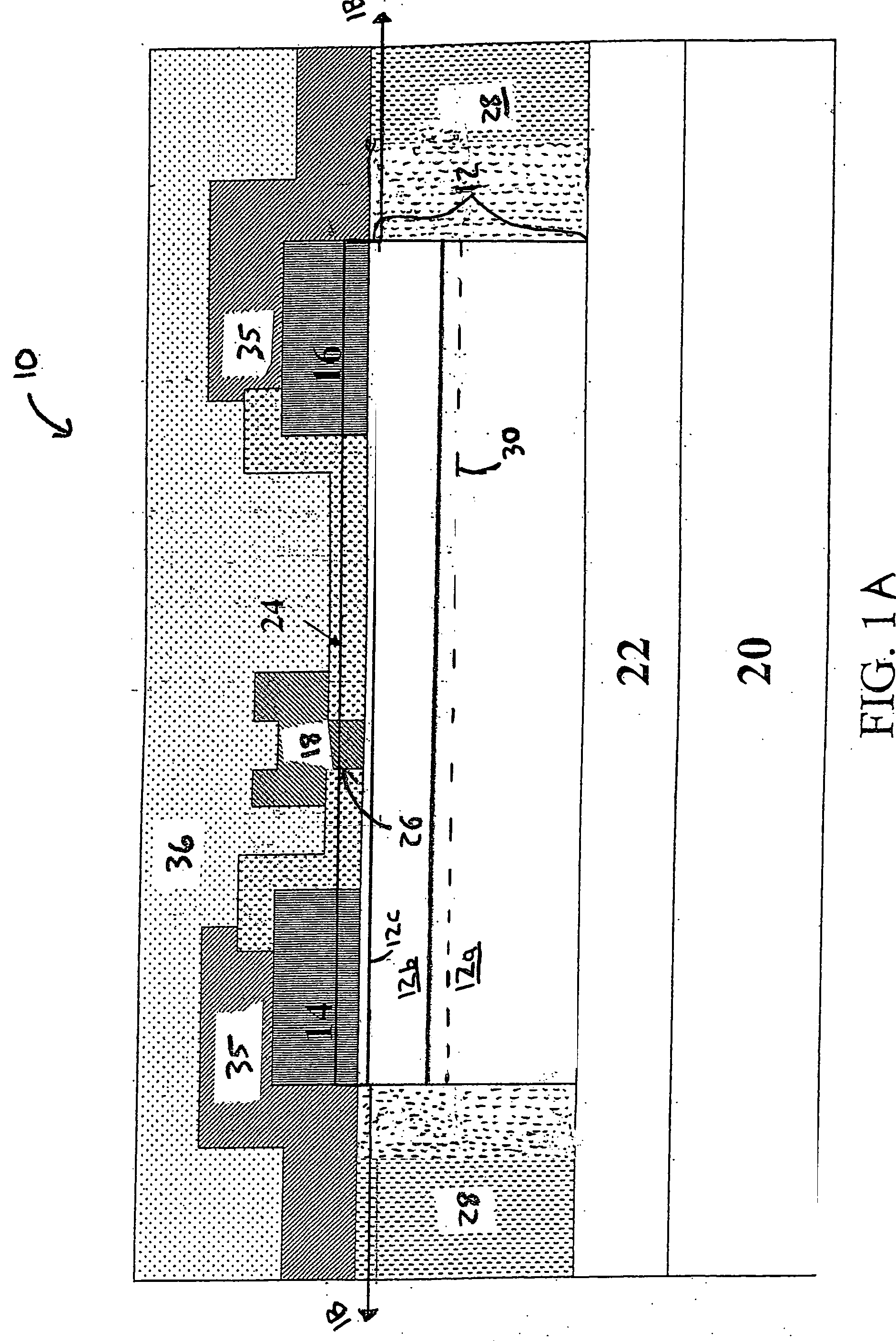
[0093] This example describes production and characterization of HFET devices that include a gallium nitride material device region. An isolation region is formed in the gallium nitride material region.

[0094] All structural layers in this example were grown by MOCVD using conventional precursors in a cold-wall, rotating disc reactor designed from flow dynamic simulations. The process used high-resistivity 100 mm Si (111) wafers as substrates. An aluminum nitride layer having a thickness of about 400 nm was grown on the surface of the substrate. It is believed that a very thin (e.g., about 20 Angstroms) amorphous silicon nitride layer may be formed between the aluminum nitride layer and the silicon substrate.. A compositionally graded AlxGa(1−x)N transition layer was grown on the aluminum nitride layer with the value of x decreasing across from a back surface of the transition layer to a front surface of the transition layer. A UID gallium nitride (i.e., GaN) buffer layer was grown ...

example 2

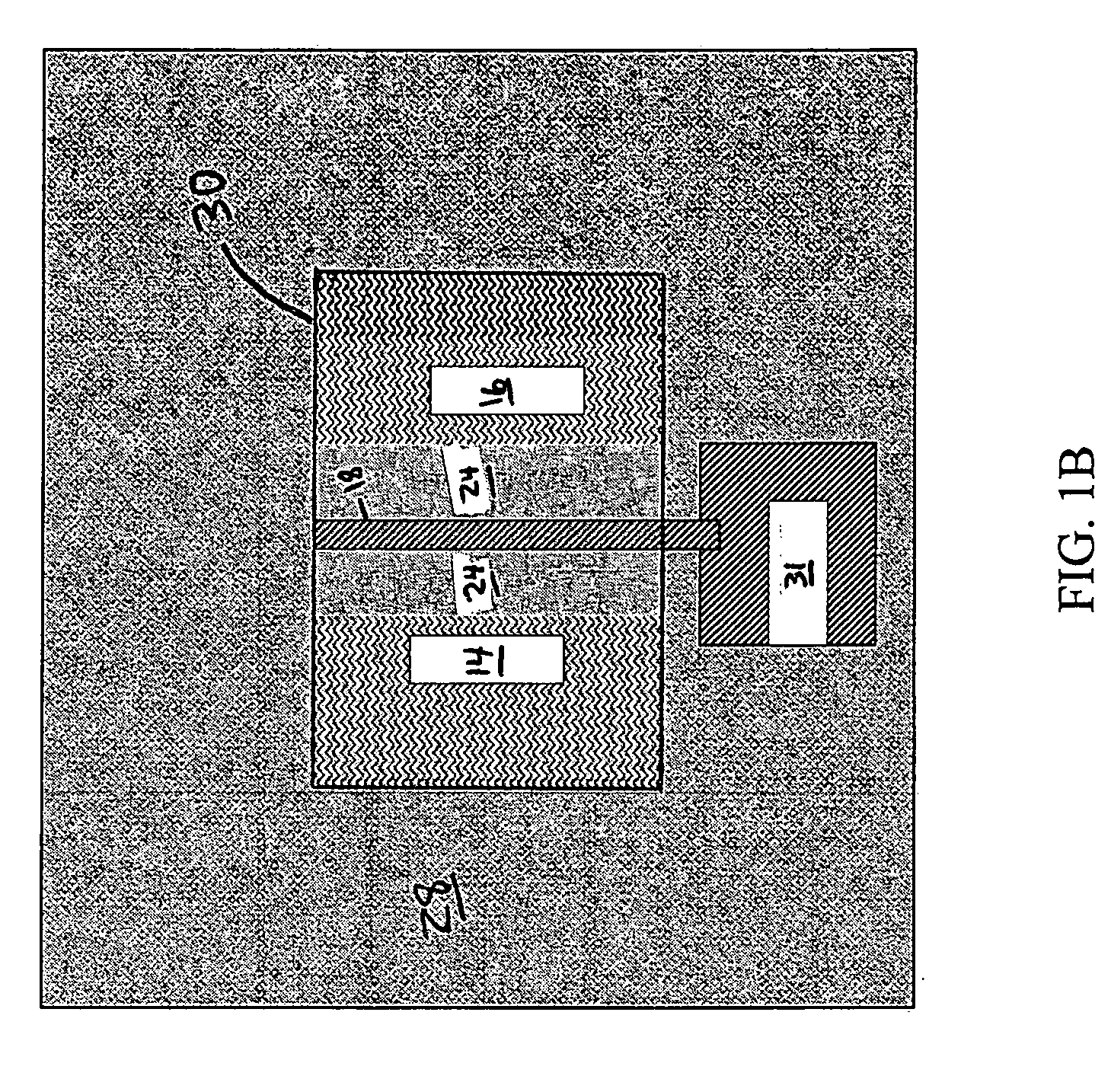
[0110] This example compares interdevice isolation current of gallium nitride material-based structures that include isolation regions of the invention to gallium nitride material-based structures that are mesa-etched for isolation. The isolation current is the current between two structures (e.g., ohmic electrodes) separated by an isolation region. Also, the effect of a SiNx passivating layer on isolation current in these structures is investigated.

[0111] Gallium nitride material-based structures were produced similar to those described in Example 1 through the ohmic metallization and rapid thermal annealing steps.

[0112] A first set of structures was processed using a mesa etching isolation process. Mesa-etched structures were produced by ICP dry etching in a BCl3 / Cl2 / Ar chemistry with a gas ratio of 8:32:10. The RF and ICP powers were 40W and 100W, respectively, and the chamber was maintained at 5 mTorr during the etch process. This recipe has been controlled to produce a smooth...

example 3

[0120] This example compares properties of gallium nitride material-based HFET devices including mesa-etched structures before, and after, an implantation step that forms an isolation region.

[0121] Gallium nitride material-based HFET structures (2×0.7 micron×50 micron) including mesa-etched isolation regions were produced, using techniques similar to those described in Example 2. HFET device fabrication then proceeded through ohmic metallization and rapid thermal annealing, gate metallization, contact pad metallization, then SiNx passivation. After passivation, leakage current of the HFET structures was characterized by current-voltage techniques. The source electrode was grounded and the gate was biased in “hard pinch-off” at −8 V. The drain voltage (Vds) was swept from 0 V to positive voltage and source, gate, and drain leakage currents were monitored as a function of Vds.

[0122] After current-voltage data were collected, the active region of the device was covered with a photore...


PUM


Abstract

Gallium nitride material structures, including devices, and methods associated with the same are provided. In some embodiments, the structures include one or more isolation regions which electrically isolate adjacent devices. One aspect of the invention is the discovery that the isolation regions also can significantly reduce the leakage current of devices (e.g., transistors) made from the structures, particularly devices that also include a passivating layer formed on a surface of the gallium nitride material. Lower leakage currents can result in increased power densities and operating voltages, amongst other advantages.

Description

RELATED APPLICATIONS [0001] This application is a continuation-in-part of U.S. patent application Ser. No. 10 / 740,376, filed Dec. 17, 2003, and entitled “Gallium Nitride Material Devices Including An Electrode-Defining Layer and Methods of Forming the Same”, the disclosure of which is incorporated herein by reference.FIELD OF INVENTION [0002] The invention relates generally to gallium nitride materials and, more particularly, to gallium nitride material structures that include isolation regions and methods associated with the same. BACKGROUND OF INVENTION [0003] Gallium nitride materials include gallium nitride (GaN) and its alloys such as aluminum gallium nitride (AlGaN), indium gallium nitride (InGaN), and aluminum indium gallium nitride (AlInGaN). These materials are semiconductor compounds that have a relatively wide, direct bandgap which permits highly energetic electronic transitions to occur. Gallium nitride materials have a number of attractive properties including high elec...

Claims


Application Information

Patent Timeline
IPC IPC(8): H01L21/285H01L21/329H01L21/335H01L29/20H01L29/872
CPCH01L21/28587H01L21/7605H01L29/2003H01L29/872H01L29/66462H01L29/7787H01L29/66212
Inventor JOHNSON, JERRY W.BORGES, RICARDOBROWN, JEFFREY D.COOK, JAMES W. JR.HANSON, ALLEN W.PINER, EDWIN L.RAJAGOPAL, PRADEEPROBERTS, JOHN C.SINGHAL, SAMEERTHERRIEN, ROBERT J.VESCAN, ANDREI
Owner NITRONEX
Why Eureka
Try Eureka