Single longitudinal mode laser diode

Active Publication Date: 2005-07-07
MACOM TECH SOLUTIONS HLDG INC
View PDF16 Cites 32 Cited by
  • Summary
  • Abstract
  • Description
  • Claims
  • Application Information

AI Technical Summary

Benefits of technology

[0009] The foregoing structure and fabrication method provide a cost-effective solution for producing single mode laser diodes with a high SMSR. The devices so fabricated are single mode lasers that are stable for a wide t

Problems solved by technology

The sub-micron e-beam or focused ion beam lithography processes used for DBR lasers are not desirable for mass production because of their serial nature, and the delicate crystal re-growth processes needed to fabricate the corrugated surface in DFB lasers make them unsuitable.
These sophisticated processes inevitably give low yield and high cost for the production of these lasers, so there has been a strong demand for more cost-effective single mode lasers, especially for use in the growing fields of data-communications.
In addition, VCSELs suffer from their inability

Method used


Image

  • Single longitudinal mode laser diode
  • Single longitudinal mode laser diode
  • Single longitudinal mode laser diode

Examples


first embodiment

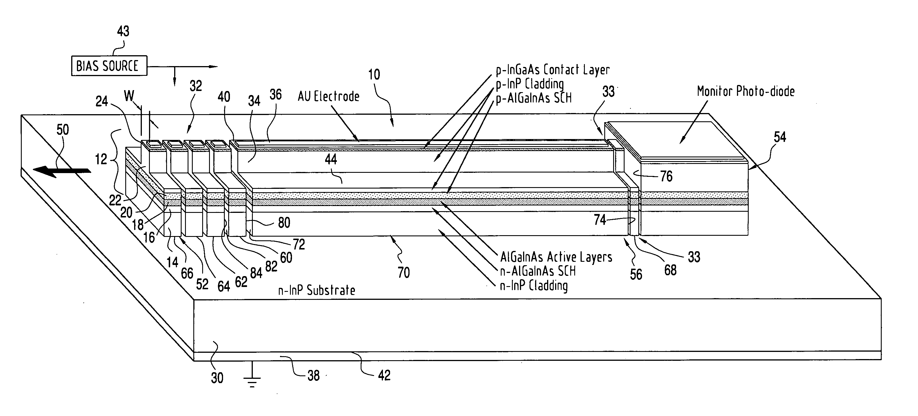
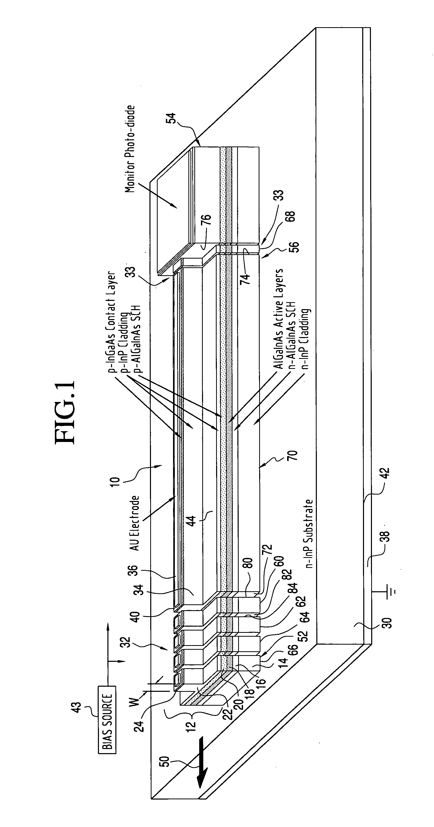
[0023] In a device constructed in accordance with this first embodiment, the wafer 12 was fabricated with an n-InP cladding layer 14, an n-AlGaInAs SCH (separate confinement heterostructure) layer 16, AlGaInAs strained multi-quantum well active layers 18, a p-AlGaInAs SCH layer 20, a p-InP cladding layer 22 and a highly doped p-InGaAs contact layer 24, formed successively on an n-type (100) InP wafer 30. The active region 18 consisted of, for example, six 6 nm compressively strained AlGaInAs quantum wells separated by 10 nm tensile-strained AlGaInAs barrier layers; the band gap of the quantum well was about 1300 nm.

[0024] The laser 10 was formed from the epitaxial wafer 12 by two steps of chemically-assisted ion-beam etching (CAIBE), which were carried out using an SiO2 mask, patterned by lithography in conventional manner. Multiple blocks 32 and 33 (to be described) were formed along the longitudinal axis of the laser 10, at its front and back ends, respectively, by the first CAIBE...

second embodiment

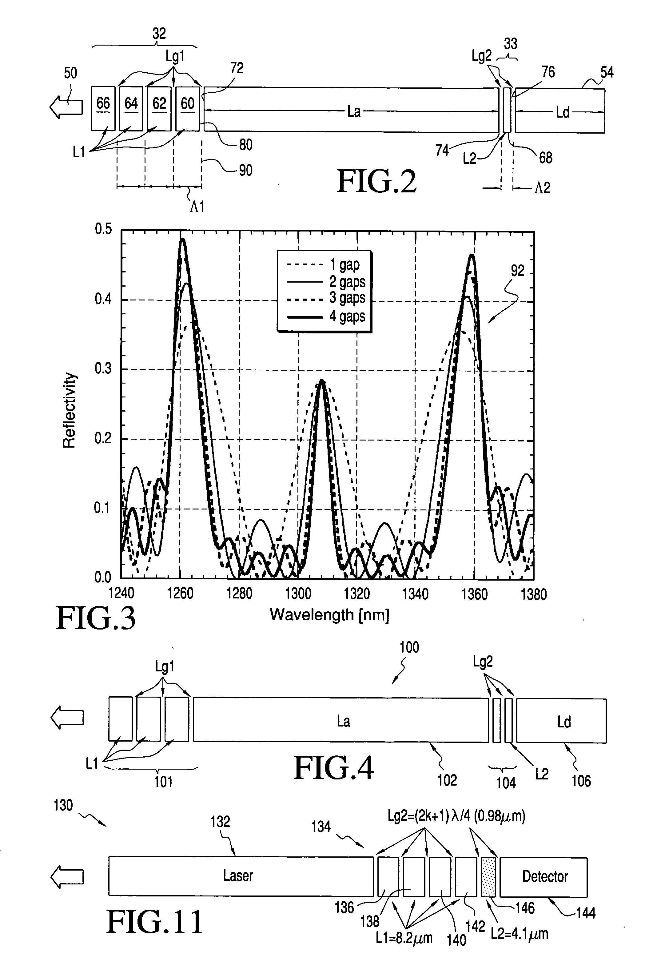
[0033]FIG. 4 is a one-dimensional schematic diagram of the present invention. In this embodiment, the laser 100 includes a front reflector 101 having three elements, a main cavity 102, a rear reflector 104, and a monitor 106. The specific parameters of a device fabricated in accordance with this configuration were N=3, L1=8.06 μm, Lg=1.31 μm, M=2, L2=4.08 μm, Lg2=0.98 μm, La=200 μm and Ld=100 μm. In this design, the FSR of the front reflector structure 100 was ˜28 nm. With these parameters, a mode jump into the neighboring filter peak will occur every 70 deg. C., because the temperature dependence of the gain peak and the resonant mode are 0.5 nm / C and 0.1 nm / C, respectively. This is not good enough for an uncooled device, which is expected to be single mode operation in the temperature range 0-85deg.C. Accordingly, the rear DBR reflector 104 was carefully designed to give reflection dips on the neighboring filter peaks of the front FP structures in order to suppress the mode jump. ...

third embodiment

[0040]FIG. 11 illustrates at 130 the invention, wherein the front reflector stack for the laser cavity 132 is eliminated, and wherein a rear stack 134 includes four high-reflection FP elements 136, 138, 140 and 142, each having a length L1 of about 8.2 μm forming a narrow-band stacked FP filter. Between the stack 134 and a monitor photodetector 144, is a narrow FP filter element 146 having a length L2 equal to about 4.1 μm. The gaps Lg2 between the filter elements have a width of (2k+1)λ / 4, where k is an integer, or in this embodiment, about 0.98 μm. The quarter-wave gaps provide a narrow band, high reflection filter that results in higher slope efficiency.


PUM


Abstract

A single-mode, etched facet distributed Bragg reflector laser includes an AlGaInAs/InP laser cavity, a front mirror stack with multiple Fabry-Perot elements, a rear DBR reflector, and a rear detector. The front mirror stack elements and the rear reflector elements include input and output etched facets, and the laser cavity is an etched ridge cavity, all formed from an epitaxial wafer by a two-step lithography and CAIBE process.

Description

[0001] This application claims the benefit of U.S. Provisional Application No. 60 / 499,340, filed Sep. 3, 2003, the disclosure of which is hereby incorporated herein by reference.BACKGROUND OF THE INVENTION [0002] The present invention relates, in general, to improved single longitudinal mode laser diodes and to methods for producing the same. [0003] Single mode lasers with a high side-mode suppression ratio (SMSR) are key devices for many applications, including, for example, spectroscopy, sensing and optical communications. To date, so-called distributed feedback (DFB) lasers, distributed Bragg reflector (DBR) lasers, and vertical cavity surface-emitting lasers (VCSEL) have been exclusively used for such applications. However, the fabrication of laterally coupled DBR lasers and the fabrication of buried hetero-structure DFB lasers require the use of sophisticated fabrication techniques. The sub-micron e-beam or focused ion beam lithography processes used for DBR lasers are not desi...

Claims


Application Information

Patent Timeline
IPC IPC(8): G02B5/28H01SH01S3/03H01S3/08H01S5/00H01S5/026H01S5/0625H01S5/10H01S5/125H01S5/14H01S5/22H01S5/343
CPCB82Y20/00H01S5/0264H01S5/0625H01S5/06256H01S5/0655H01S5/1017H01S5/34313H01S5/1039H01S5/125H01S5/141H01S5/22H01S5/343H01S5/1021
Inventor BEHFAR, ALEX A.MURO, KIYOFUMISTAGARESCU, CRISTIAN B.SCHREMER, ALFRED T.
Owner MACOM TECH SOLUTIONS HLDG INC
Why Eureka
Try Eureka