Micro-engineered electron multipliers

a micro-engineered, electron-producing technology, applied in the direction of multiplier electrode arrangements, multiplier tubes, instruments, etc., can solve the problems of limited range of possible features, high cost of processing, and restricted choice of coatings for secondary electron emission, so as to enhance secondary electron emission

Active Publication Date: 2005-07-14
MICROSAIC SYST
View PDF8 Cites 6 Cited by
  • Summary
  • Abstract
  • Description
  • Claims
  • Application Information

AI Technical Summary

Benefits of technology

[0014] This invention provides for a simple method of fabricating miniature electron multipliers in an in-plane configuration for use with miniature analytic instruments such as mass filters. The materials involved are predominantly silicon and compatible oxides, thereby allowing the possibility of integration with a mass filter formed in a similar materials system. The materials are selected simulta

Problems solved by technology

Features with arbitrary shapes may be formed, in an orientation normal to the substrate plane; however, the process is expensive, and the features are formed in non-silicon materials such as electroplated metal.
Although these materials can be modified with additional surface coatings, the choice of coatings that may be used for secondary electron emission is restricted.
However, the range of possible features is limited, because the process forms structures that are bounded by specific crystal planes (typically, the plane).
As a result, it is not possible to form arbitrar

Method used


Image

  • Micro-engineered electron multipliers
  • Micro-engineered electron multipliers
  • Micro-engineered electron multipliers

Examples


Embodiment Construction

[0054] A detailed description of the invention is now provided, with reference to FIGS. 1-5.

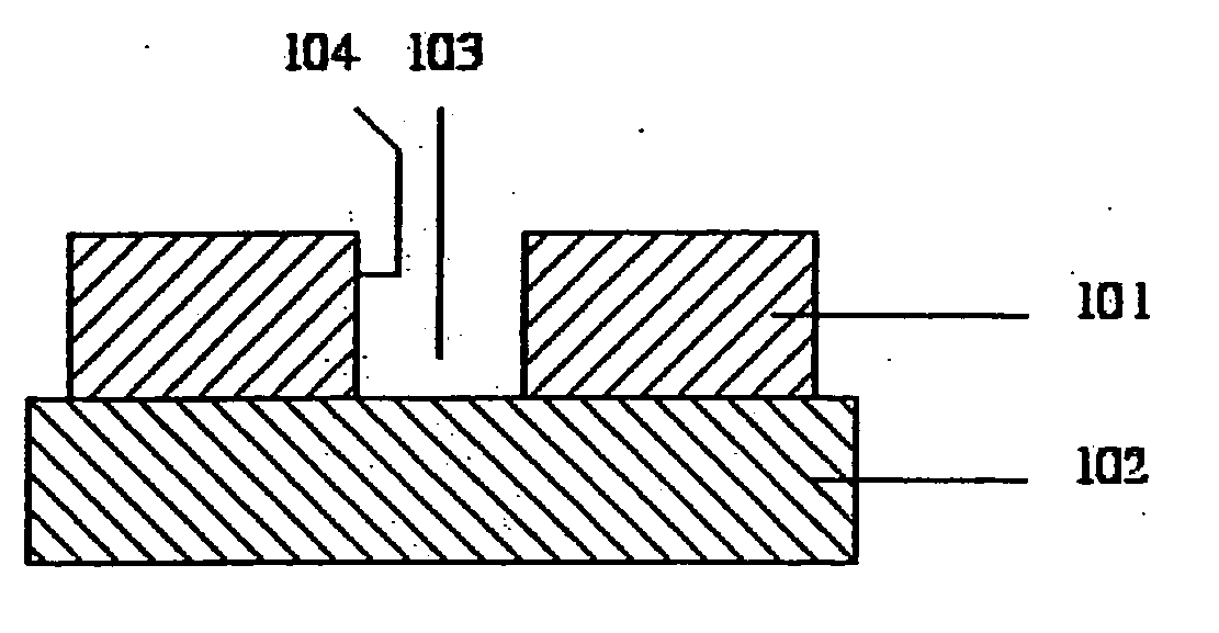
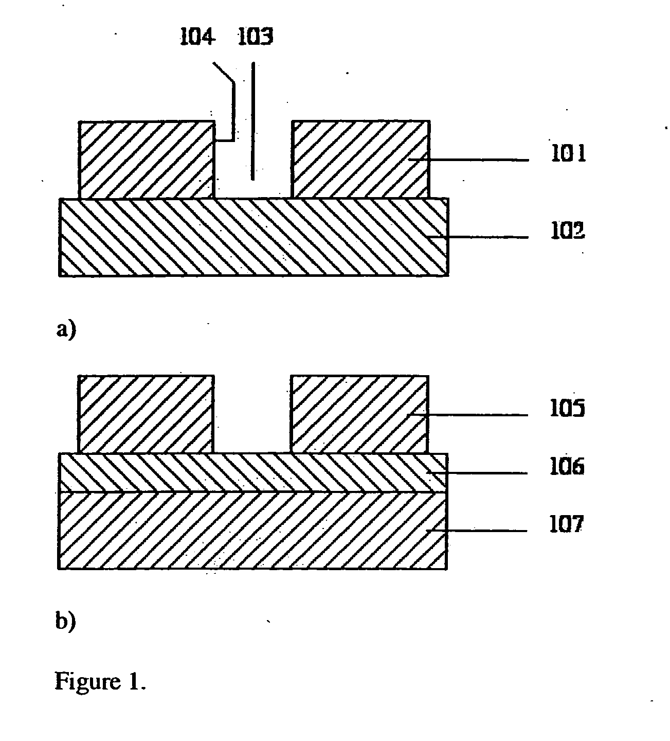
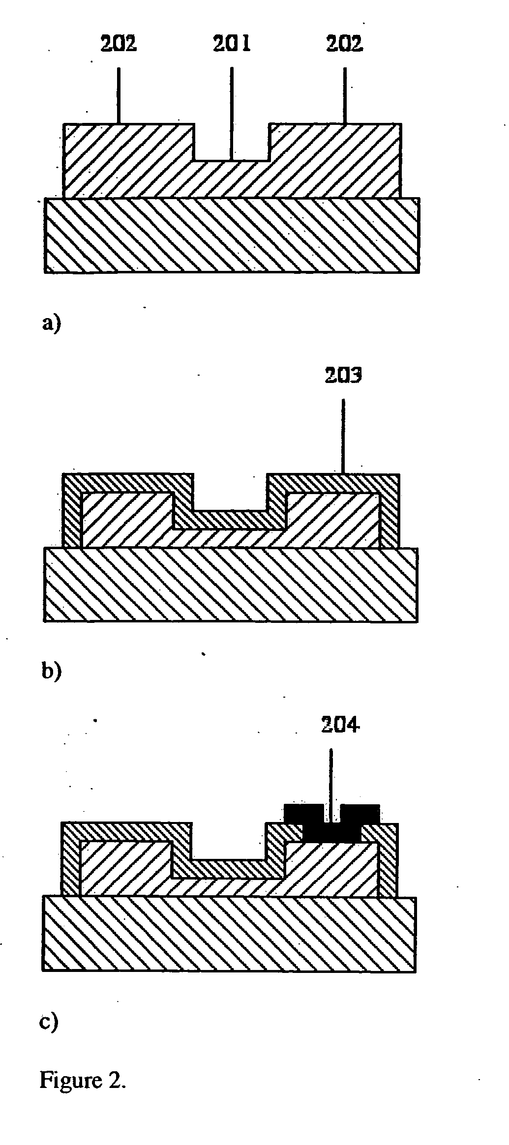
[0055]FIG. 1a shows a cross-section of a silicon-on-glass wafer, which consists of a first material provided by a silicon layer 101 bonded to a second material provided by a glass or silica layer 102. The first material is a semiconductor, which may be converted into an insulator with enhanced secondary emission properties by oxidation and subsequent annealing at high temperature in hydrogen gas. It will be appreciated that in this context, the hydrogen is acting as a reducing agent and that other reducing agents could equivalently be used for specific applications. The second layer provides an insulating substrate. Using a single layer of patterning, the silicon layer 101 may be structured by deep reactive ion etching (DRIE) to form vertical features 103, stopping at the interface between the two materials. It will be appreciated that each vertical feature forms a structure with sidewalls 1...


PUM


Abstract

This invention provides for a simple method of fabricating miniature electron multipliers, in an in-plane configuration suitable for use with miniature analytic instruments such as mass filters. The materials involved are predominantly silicon and compatible oxides, allowing the possibility of integration with a mass filter formed in a similar materials system. The materials are selected simultaneously to withstand high voltages and to. enhance secondary electron emission. Fabrication is based on standard planar processing methods. These methods also allow the construction of an integrated set of bias resistors in a multi-electrode device, so that the device may be operated from a single high-voltage source.

Description

FIELD OF THE INVENTION [0001] The invention relates to electron multipliers and particularly to electron multipliers formed in a Microelectromechanical system (MEMS) environment. BACKGROUND [0002] Originally developed for early TV cameras, electron multipliers are of considerable importance in low-signal light detection, night vision and mass spectrometry, and in instrumentation for high-energy physics. They provide an analogous function to the erbium doped fibre amplifier in optical communications, namely low-noise, high gain pre-detector amplification. There are a wide variety of different configurations, including discrete dynode devices and mesh multipliers, and continuous dynode devices such as microchannel plates and channeltron multipliers. Variants such as the Gas Electron Multiplier (GEM) are used for particle detection. Some types (e.g. microchannel plates) amplify photoelectrons from an image, while others (e.g. channeltrons) are single-channel devices for instrumentation...

Claims


Application Information

Patent Timeline
IPC IPC(8): H01J9/12H01J40/14H01J43/22
CPCH01J9/125H01J43/246H01J43/22
Inventor SYMS, RICHARD
Owner MICROSAIC SYST
Why Eureka
Try Eureka