Method of fabricating lanthanum oxide layer and method of fabricating MOSFET and capacitor using the same

a technology of lanthanum oxide and mosfet, which is applied in the field of methods of fabricating mosfet and capacitors using the same, and methods of fabricating lanthanum oxide layers. it can solve the problems of increased leakage current, unsuitable dielectric layers for use in semiconductor devices, and increased leakage current, so as to improve the layer formation productivity

Active Publication Date: 2005-07-21
SAMSUNG ELECTRONICS CO LTD
View PDF5 Cites 40 Cited by
  • Summary
  • Abstract
  • Description
  • Claims
  • Application Information

AI Technical Summary

Benefits of technology

[0011] Accordingly, the present invention is generally directed to methods of fabricating a lanthanum oxide dielectric layer for use in an improved semiconductor device, the methods having the characteristic of an improved layer formation productivity by using an appropriate precursor.

Problems solved by technology

However, the approach of reducing a thickness of the dielectric layer may lead to an undesirable increase in leakage current as the dielectric layer thickness is reduced.
However, even though a new dielectric layer may have a desirably high dielectric constant, such a dielectric layer may not be suitable for use in a semiconductor device.
First, use of a BST layer, a titanium oxide layer, a tantalum oxide layer, and the like may result in an increase of a leakage current, a degradation of a carrier mobility, and / or similar interface problems because interface characteristics can deteriorate due to a high reactivity of the high-k layers with a silicon substrate.
On the other hand, in the case of using an aluminum oxide layer, the aluminum oxide layer has a relatively excellent thermal stability, but its use as a dielectric layer is limited due to its relatively low dielectric constant.
Further, aluminum oxide has a disadvantage in that it creates a difficulty in controlling a threshold voltage due to a negative fixed charge.
Furthermore, the use of a hafnium oxide layer or a zirconium oxide layer is also limited because such materials may be crystallized during an annealing step of subsequent semiconductor fabrication processes, thereby increasing a leakage current.
In addition to the above-described problems, efforts to apply the high-k and ultra high-k dielectric layers to the capacitor dielectric layer may cause further problems as follows.
Even though the BST layer and the PZT layer have ultra high dielectric constants, such layers are difficult to form with a uniform composition on a lower electrode structure having a high aspect ratio.
The use of a high-k tantalum oxide layer is also limited because of the tendency to cause a high leakage current when used with a lower electrode consisting of a polysilicon layer due to a low conduction band offset at the polysilicon layer interface.
Further, the use of a zirconium oxide layer or a hafnium oxide layer may cause a rapid increase in a leakage current during a subsequent annealing process step because these materials have relatively low crystallization temperatures.
An aluminum oxide layer has the advantages of a relatively high conduction band offset at a polysilicon interface as well as a high crystallization temperature and an excellent step coverage, but it has a limited ability to increase a capacitance of a capacitor due to having a relatively low dielectric constant.
However, the compound La(thd)3 which is employed as a lanthanum precursor in these patents may not be suitable for actual commercial applications because of productivity and / or economic performance, or other operational limitations due to such process requirements as a low vapor pressure, a high process temperature, a low growth rate, or the like in comparison with the processes employed for forming other types of dielectric layers.

Method used


Image

  • Method of fabricating lanthanum oxide layer and method of fabricating MOSFET and capacitor using the same
  • Method of fabricating lanthanum oxide layer and method of fabricating MOSFET and capacitor using the same
  • Method of fabricating lanthanum oxide layer and method of fabricating MOSFET and capacitor using the same

Examples


Embodiment Construction

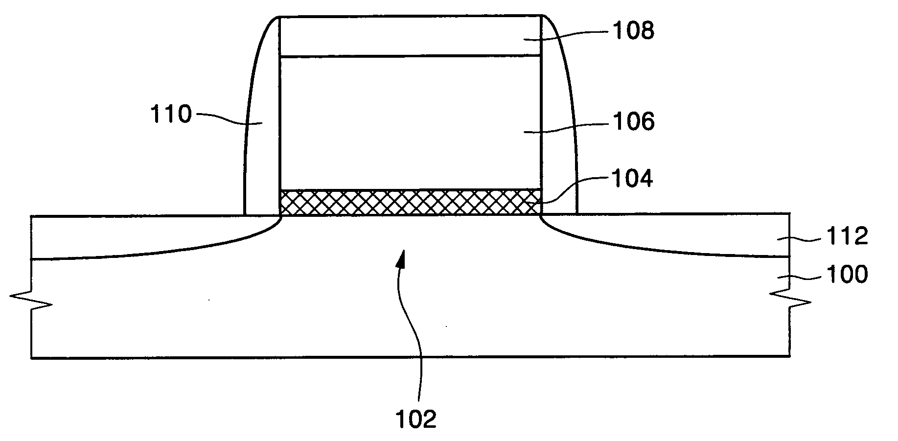
[0028] The present invention will now be described more fully hereinafter with reference to the accompanying drawings, in which preferred embodiments of the invention are shown. It will be understood, however, that this invention may be embodied in many different forms and should not be construed as being limited to the embodiments set forth herein. Rather, these embodiments are provided so that this disclosure will be thorough and complete, and will fully convey the scope of the invention to those skilled in the art. In the drawings, the thicknesses of layers and regions are exaggerated for clarity. Like numbers refer to like elements throughout the specification.

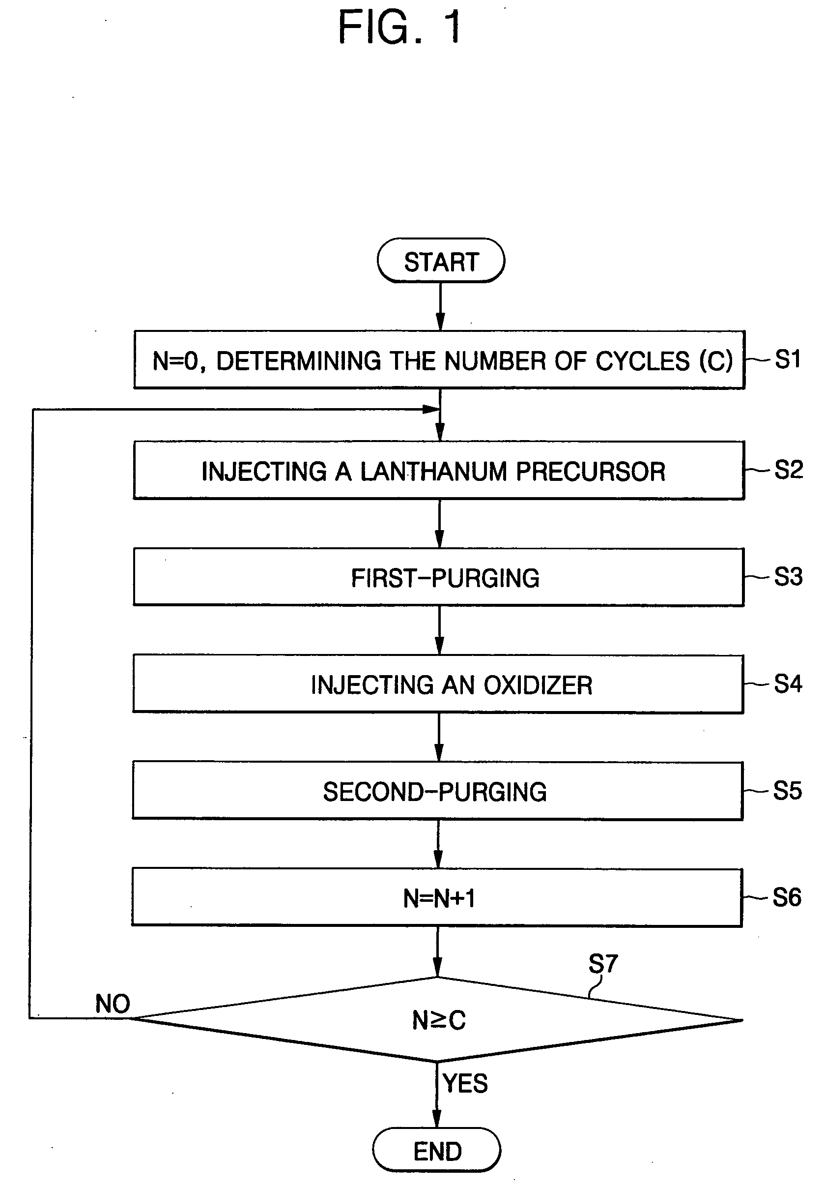
[0029]FIG. 1 is a process flow chart illustrating the sequential steps in a method of fabricating a lanthanum oxide layer according to an embodiment of the present invention.

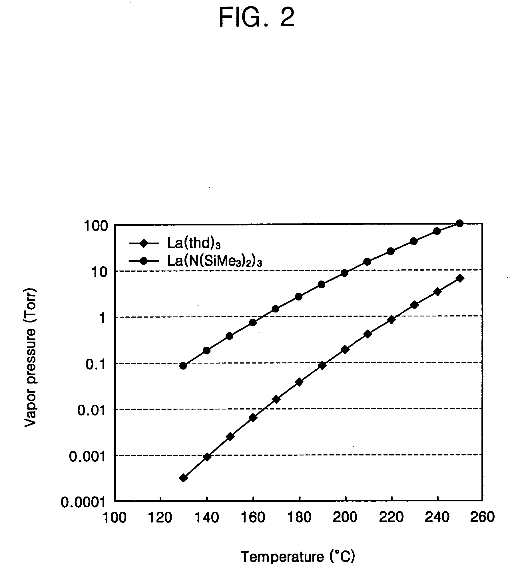
[0030] An atomic layer deposition (ALD) method is a preferred technique used in the method of fabricating a lanthanum oxide layer according to an em...


PUM

PropertyMeasurementUnit
pressureaaaaaaaaaa
temperatureaaaaaaaaaa
dielectric constantaaaaaaaaaa

Abstract

Methods of fabricating a lanthanum oxide layer, and methods of fabricating a MOSFET and/or a capacitor especially adapted for semiconductor applications using such a lanthanum oxide layer are disclosed. The methods include a preliminary step of disposing a semiconductor substrate into a chamber. Tris(bis(trimethylsilyl)amino)Lanthanum as a lanthanum precursor is then injected into the chamber such that the lanthanum precursor is chemisorbed on the semiconductor substrate. Then, after carrying out a first purge of the chamber, at least one oxidizer is injected into the chamber such that the oxidizer is chemisorbed with the lanthanum precursor on the semiconductor substrate. Then, the chamber is purged a second time. The described steps of injecting the lanthanum precursor into the chamber, first-purging the chamber, injecting an oxidizer into the chamber, and second-purging the chamber may be sequentially and repeatedly performed to form a lanthanum oxide layer of a desired thickness having enhanced semiconductor characteristics.

Description

CROSS-REFERENCE TO RELATED APPLICATION [0001] This application claims the benefit of Korean Patent Application No. 2004-0002453, filed Jan. 13, 2004, the disclosure of which is hereby incorporated herein by reference in its entirety. BACKGROUND [0002] 1. Technical Field [0003] The present invention relates to methods of fabricating a dielectric layer and methods of fabricating a semiconductor device using the same, and more particularly, to methods of fabricating a lanthanum oxide layer, and methods of fabricating a MOSFET and a capacitor using the same. [0004] 2. Discussion of the Related Art [0005] In a semiconductor memory device, a dielectric layer is used for various applications, and is generally used for a capacitor dielectric layer or a gate dielectric layer of a MOSFET. In order to operate a semiconductor device in a normal way, the gate dielectric layer or a capacitor dielectric layer should maintain an appropriate level of capacitance C. A capacitance C of a dielectric la...

Claims


Application Information

Patent Timeline
Patent Type & Authority Applications(United States)
IPC IPC(8): C23C16/40H01L21/31H01L21/314H01L21/316
CPCC23C16/40H01L21/28194H01L29/517H01L21/31604H01L21/3141H01L21/02192H01L21/02175H01L21/0228H01L21/022F21V17/12F21W2131/101
Inventor KIM, JONG-PYOLEE, JUNG-HYUNSEO, BUM-SEOKLEE, JUNG-HYOUNG
Owner SAMSUNG ELECTRONICS CO LTD
Why Eureka
Try Eureka