Capacitor of a semiconductor device, memory device including the same and method of munufacturing the same

a semiconductor and memory technology, applied in the field of semiconductor devices, can solve the problems of loss of stored data when power is turned off, different properties of ferroelectric capacitor dielectric film, and very rough surface of pzt film, so as to reduce the surface roughness of ferroelectric film, reduce leakage current, and easy growth

Inactive Publication Date: 2005-07-28
SAMSUNG ELECTRONICS CO LTD
View PDF11 Cites 14 Cited by
  • Summary
  • Abstract
  • Description
  • Claims
  • Application Information

AI Technical Summary

Benefits of technology

[0035] The lower electrode according to an embodiment of the present invention acts as a strong diffusion barrier, reducing a leakage current at an interface between the lower electrode and the ferroelectric film. Also, a crystal nucleus of the ferroelectric film can be easily grown and surface roughness of the ferroelectric film can be reduced. Further, since a wide process window for the ferroelectric film can be secured, the ferroelectric film can be formed under a variety of process conditions.
[0036] Since a strong diffusion barrier function and a wide process window are obtained, reproducibility, reliability, and yield of the capacitor can be increased. In addition, physical properties, such as fatigue characteristics and a data retention characteristic, can be improved.

Problems solved by technology

DRAM and static random access memory (SRAM) offer advantages of higher integration densities and faster data processing speeds than nonvolatile memory devices, such as flash memory, but also have a disadvantage of losing stored data when power is turned off.
However, the properties of the dielectric film of a ferroelectric capacitor are different from the properties of the dielectric film of a general semiconductor capacitor.
Second, the PZT film has a very rough surface.
Third, there is a large leakage current at an interface between the lower electrode and the PZT film.

Method used


Image

  • Capacitor of a semiconductor device, memory device including the same and method of munufacturing the same
  • Capacitor of a semiconductor device, memory device including the same and method of munufacturing the same
  • Capacitor of a semiconductor device, memory device including the same and method of munufacturing the same

Examples


Embodiment Construction

[0064] Korean Patent Application No. 10-2004-0004681, filed on Jan. 26, 2004, in the Korean Intellectual Property Office, and entitled: “Capacitor of Semiconductor Device, Memory Device Comprising the Same and Method of Manufacturing the Same,” is incorporated by reference herein in its entirety.

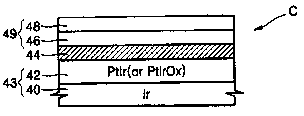
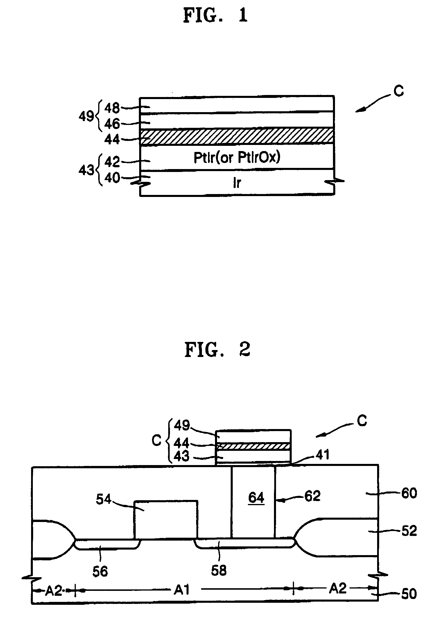
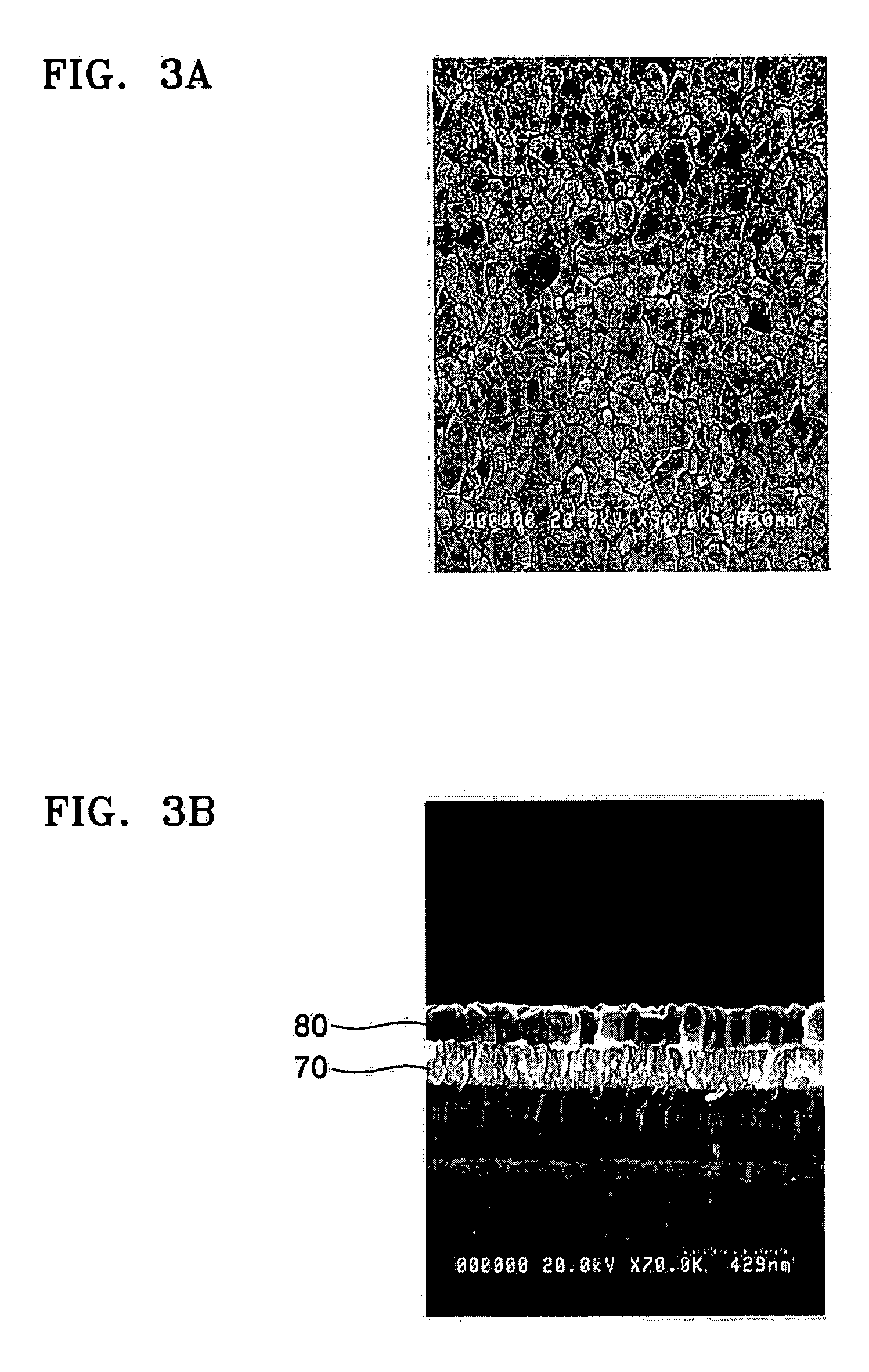
[0065] The present invention will now be described more fully hereinafter with reference to the accompanying drawings, in which exemplary embodiments of the invention are shown. This invention may, however, be embodied in different forms and should not be construed as limited to the embodiments set forth herein. Rather, these embodiments are provided so that this disclosure will be thorough and complete, and will fully convey the scope of the invention to those skilled in the art. In the drawing figures, the dimensions of layers and regions are exaggerated for clarity of illustration. It will be understood that when an element such as a layer, region or substrate is referred to as being “on...


PUM

PropertyMeasurementUnit
thicknessaaaaaaaaaa
thicknessaaaaaaaaaa
thicknessaaaaaaaaaa

Abstract

In a capacitor, a memory device including the capacitor, and a method of manufacturing the capacitor, the capacitor includes a lower electrode comprising a single layer of one selected from the group including a noble metal alloy and an oxide thereof, a dielectric film formed on the lower electrode, and an upper electrode formed on the dielectric film.

Description

BACKGROUND OF THE INVENTION [0001] 1. Field of the Invention [0002] The present invention relates to a semiconductor device and a method of manufacturing the same. More particularly, the present invention relates to a capacitor having increased reproducibility, reliability, and yield, a memory device including the capacitor, and a method of manufacturing the capacitor. [0003] 2. Description of the Related Art [0004] A capacitor of a semiconductor device includes a lower electrode, a dielectric film, and an upper electrode, and is commonly used as a data storage medium for a semiconductor memory device, such as a dynamic random access memory (DRAM). [0005] DRAM and static random access memory (SRAM) offer advantages of higher integration densities and faster data processing speeds than nonvolatile memory devices, such as flash memory, but also have a disadvantage of losing stored data when power is turned off. [0006] Therefore, memory devices that have the advantages of volatile memo...

Claims


Application Information

Patent Timeline
Patent Type & Authority Applications(United States)
IPC IPC(8): H01L21/02H01L27/105H01L21/8242H01L21/8246
CPCH01L27/10852H01L28/65H01L28/55H10B12/033H01L27/105
Inventor SHIN, SANG-MINKOO, JUNE-MOKIM, SUK-PILCHO, CHOONG-RAE
Owner SAMSUNG ELECTRONICS CO LTD
Why Eureka
Try Eureka