Method for etching a quartz layer in a photoresistless semiconductor mask

a technology of photoresistless semiconductor and quartz layer, which is applied in the field of integrated circuits, can solve the problems of reducing the feature contrast during subsequent semiconductor wafer fabrication, difficult to precisely control the etching depth of quartz layer, and etching applied to cpl

Active Publication Date: 2005-07-28
NXP USA INC
View PDF5 Cites 42 Cited by
  • Summary
  • Abstract
  • Description
  • Claims
  • Application Information

AI Technical Summary

Problems solved by technology

These shortcomings include a fast quartz layer etch rate that makes it difficult to precisely control etching depth in the quartz layer.
An incorrect depth in the quartz layer will result in incorrect shifting and ultimately reduce the feature contrast during subsequent semiconductor wafe

Method used


Image

  • Method for etching a quartz layer in a photoresistless semiconductor mask
  • Method for etching a quartz layer in a photoresistless semiconductor mask
  • Method for etching a quartz layer in a photoresistless semiconductor mask

Examples


Embodiment Construction

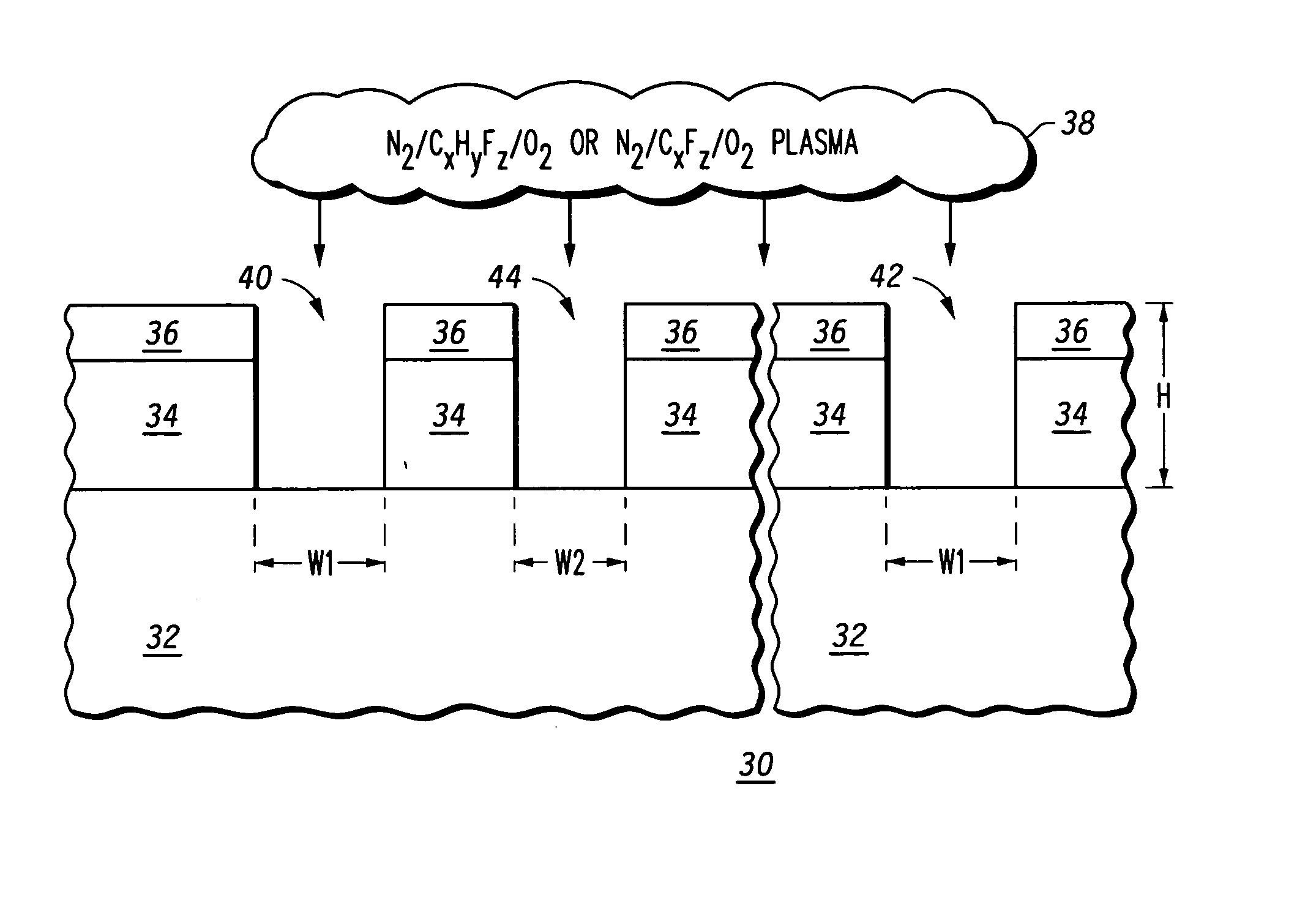
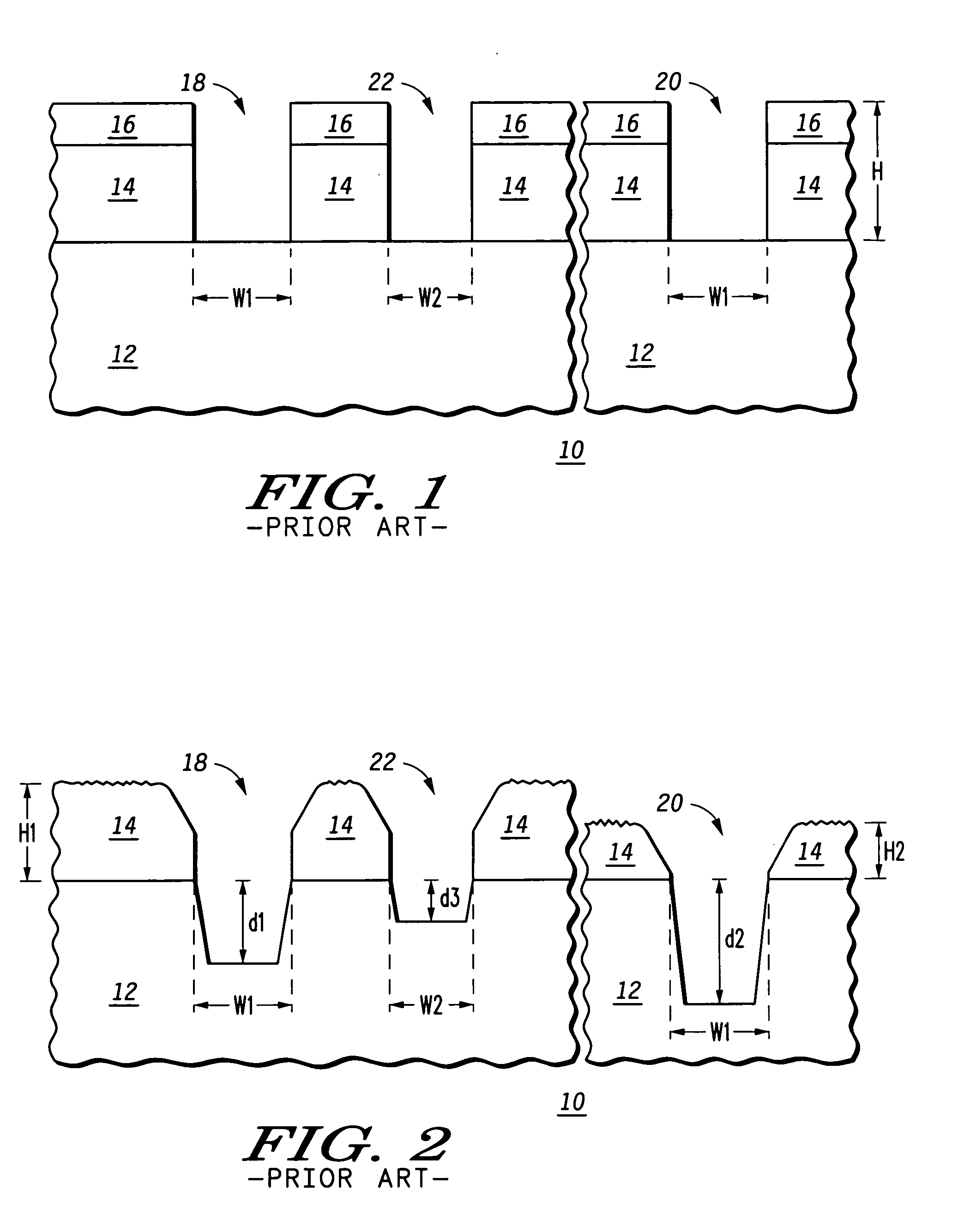
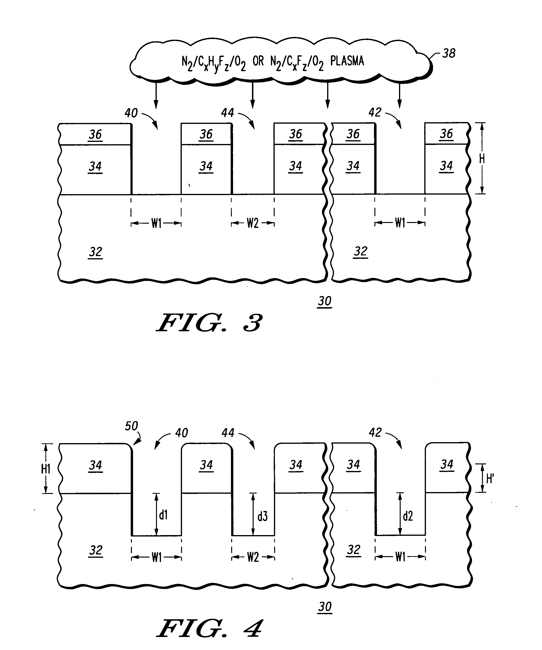
[0011] Illustrated in FIG. 1 is a cross-section of a known mask 10. A quartz substrate 12 has formed thereon a chrome (Cr) layer 14. Overlying the chrome layer 14 is a chrome oxynitride (CrOxNy) layer 16. Openings 18 and 20 having a width W1 have been etched into the mask 10 using a halogen based plasma (e.g. chlorine based). The openings 18 and 20 are in separate areas of the mask 10 as noted by the break in mask 10. Additionally shown is an opening 22 having a width W2 that is less than W1. Because chrome layer 14 and the CrOxNy layer 16 are thin, the sidewalls of the opening are substantially vertical. Additionally, halogen based metal etching plasmas are not highly polymerizing and are mainly ion driven. Therefore, there is a thin passivation layer (not illustrated) on the sidewalls that do not inhibit ion etching. As used herein, the term “quartz” is fused quartz that is crystal quartz that is melted at a white heat and cooled to form an amorphous glass. It is not birefringemen...


PUM

PropertyMeasurementUnit
Fractionaaaaaaaaaa
Fractionaaaaaaaaaa
Fractionaaaaaaaaaa

Abstract

A chromeless phase lithography mask (30) that does not require photoresist to manufacture has a quartz substrate (32) is etched by using a plasma (38) containing one of a nitrogen augmented hydro-fluorocarbon oxygen mixture and a nitrogen augmented fluorocarbon oxygen mixture. Various hydro-fluorocarbons or fluorocarbons may be used. The nitrogen addition results in etched openings in the quartz substrate that have substantially vertical sidewalls in a uniform manner across the substrate. Surface roughness is minimized and edges of the openings are well-defined with minimal rounding. The etch rate is rendered controllable by reducing bias power without degrading a desired vertical sidewall profile.

Description

FIELD OF THE INVENTION [0001] This invention relates generally to integrated circuits, and more specifically, to the manufacture of masks used to manufacture semiconductors. BACKGROUND OF THE INVENTION [0002] Phase shift mask (PSM) lithography is a known lithography technique for forming features on an integrated circuit. Photolithography requires sufficient resolution, contrast and depth of focus to form feature details having a minimum feature resolution. PSM requires etching of an underlying quartz mask plate and / or specifically deposited dielectric films to a depth that results in phase shifting of the light by a predetermined amount, typically one hundred eighty degrees. [0003] To achieve lower cost, a technique known as chromeless phase lithography (CPL) has been proposed in the literature. CPL requires fewer electron beam lithography steps, thus reducing processing costs. Quartz etching for PSM manufacturing has typically been done using fluorocarbon oxygen plasma sources. Th...

Claims


Application Information

Patent Timeline
IPC IPC(8): G03F1/00H01L21/302H01L21/311
CPCH01L21/31116G03F1/34
Inventor RAUF, SHAHIDVENTZEK, PETER L.G.WU, WEI E.
Owner NXP USA INC
Why Eureka
Try Eureka