Material supply system in semiconductor device manufacturing plant

a technology of semiconductor devices and supply systems, applied in the direction of total factory control, lapping machines, instruments, etc., can solve the problems of increasing the production cost of pure water per unit, increasing the and reducing the efficiency of processing facilities, so as to achieve the effect of efficient supply and low initial cost and running cos

Inactive Publication Date: 2005-08-11
EBARA CORP
View PDF8 Cites 23 Cited by
  • Summary
  • Abstract
  • Description
  • Claims
  • Application Information

AI Technical Summary

Benefits of technology

[0013] The present invention has been made in view of the above-mentioned problems found in the prior art, and it is an object of the invention to provide a material supply system in a semiconductor device manufacturing plant whic

Problems solved by technology

In this event, solid components in the waste water are dehydrated and wasted as sludge.
In recent years, however, semiconductor products have been increasingly required in a wider number of applications, including products for personal computers to digital electric appliances such as portable telephones, but they tend to have shorter life cycles.
In regard to a pure water supply system in the small-scaled plant, a simple reduction in scale of the pure water supply system generally installed in a large-scaled plant would cause an increase in the production cost of pure water per unit (initial cost and running cost) which is reflected to a production cost of semiconductor products.
Such problems implied in the small-scaled plant are not limited to the supply of pure water, but may apply to the supply of materials such as

Method used


Image

  • Material supply system in semiconductor device manufacturing plant
  • Material supply system in semiconductor device manufacturing plant
  • Material supply system in semiconductor device manufacturing plant

Examples


first embodiment

[0050] In the following, a pure water supply system for supplying pure water to a plurality of processing facilities will be described as a first embodiment of a material supply system in a semiconductor device manufacturing plant according to the present invention.

[0051] The inventors investigated into pure water supply systems and particularly noted the following aspects. [0052] At point of use which use pure water, every point of use requires a different quality of pure water. In other words, not all the points of use do require an ultrapure water level for the water quality. [0053] Some of points of use which use pure water require different qualities of pure water on a process-by-process basis, and do not require the ultrapure water level for the water quality in all processes. [0054] Since a small-scaled plant has a relatively small number of points of use, complicated piping is not involved in providing a plurality of quality grades for pure water and routing a pure water su...

second embodiment

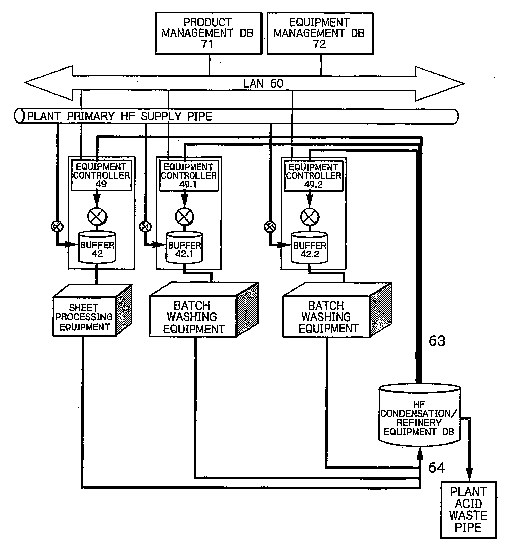
[0102]FIG. 8 illustrates a material supply system for use with a silicon film LPCVD equipment (Low Pressure Chemical Vapor Deposition) for performing an LPCVD process using a monosilane gas in accordance with a second embodiment of the present invention.

[0103] The LPCVD equipment (semiconductor manufacturing) 40, which is one of processing facilities in a semiconductor device manufacturing plant, is installed on a Fab floor within a clean room which also contains a reaction tube 41 or chamber made of highly pure quartz. The reaction pipe 41 is supplied with a monosilane gas which is a material gas for use in the LPCVD deposition, and a fluorine gas for etching silicon films deposited on the inner wall of the reaction tube 41, other contained quartz, and surfaces of parts made of silicon carbide to clean the interior of the reaction tube 41. These gases are introduced from a monosilane gas cylinder 51 installed outside the clean room and a fluorine gas generator 52 installed on the ...

third embodiment

[0125] A third embodiment will next be described in connection with an example in which a silicon film on the inner wall of the reaction tube 41 is cleaned or washed-off using a fluorine gas after a polycrystalline silicon film has been deposited using the silicon film LPCVD equipment 40 illustrated in FIG. 8 as described above.

[0126] Before the cleaning, details on cleaning and etching to be next processed by the apparatus, such as etching conditions and the like based on a current film thickness on the quartz tube, are input to the equipment controller 49 from an equipment management database 72 (FIG. 8). For example, this is peel-off of 100 nm of a polycrystalline film, which entails LPCVD deposition that is performed at 10 Torr and 300° C. for five minutes with a fluorine gas at a flow rate of 1000 sccm. The total amount of fluorine gas used in the deposition is calculated as follows:

1000 SCCM×5 minutes=5000 SCC

[0127] It is assumed that the buffer 42 has an inner volume of 50...


PUM

PropertyMeasurementUnit
Temperatureaaaaaaaaaa
Pressureaaaaaaaaaa
Concentrationaaaaaaaaaa

Abstract

In a small scaled plant intended for flexible manufacturing, a pure water supply system is provided at a low cost without reducing a production efficiency. A pure water system produces a plurality of grades of pure water which are supplied through pipes connected to points of use for cleaning, CMP, lithography, and the like. Upon receipt of a request signal from each point of use for starting to use a certain grade of pure water, a controller determines whether or not a required amount exceeds the capacity of the grade of pure water which can be supplied by the pure water system. If not, the controller sends a use permission signal to the point of use for permitting the same to use the pure water. When a certain use point is using the requested grade of pure water, the controller may not permit the requesting point of use to use the pure water until a use end signal is sent from the use point which is using the pure water.

Description

TECHNICAL FIELD OF THE INVENTION [0001] The present invention relates to semiconductor device manufacturing technologies, and more particularly to a material supply system for supplying processing facilities in a semiconductor device manufacturing plant with materials which include gases, liquids and solids. It should be first noted that the term “materials” used in this specification include gases and liquids for use in processing facilities for processing semiconductor wafers and cleaning the processing facilities themselves such as material gases and chemical, as well as gases, liquids and granular solids which are not directly used for reactions such as cooling water for pumps associated with the processing facilities, heaters for heating reaction chambers, and the like. BACKGROUND ART [0002] Conventional semiconductor device manufacturing plants are generally large in scale for relying on the mass production to reduce production costs. For example, one known manufacturing plant...

Claims


Application Information

Patent Timeline
IPC IPC(8): B24B57/02H01L21/02C11D11/00C23C16/52H01L21/00H01L21/306
CPCB24B37/04B24B57/02C11D11/0047Y10S210/90G05B2219/32082H01L21/02052H01L21/67276C23C16/52Y02P90/02
Inventor MIYAZAKI, KUNIHIRONADAHARA, SOICHIUSUDA, KINYAAKAHORI, MASAJINAKAGAWA, SOTANAKAJIMA, KEN
Owner EBARA CORP
Why Eureka
Try Eureka