Large-area nanoenabled macroelectronic substrates and uses therefor

a macroelectronic substrate and nano-enabled technology, applied in the field of nanowire thin films in semiconductor devices, can solve the problems of limited success, difficult fabrication of high-performance tfts on plastics, limited application range of current technology, etc., and achieve enhanced carrier mobility and high performance

Active Publication Date: 2005-08-18
ONED MATERIAL INC
View PDF37 Cites 164 Cited by
  • Summary
  • Abstract
  • Description
  • Claims
  • Application Information

AI Technical Summary

Benefits of technology

[0034] Systems and methods to further improve performance are described herein, according to further aspects of the present invention. For example, aspects of the present invention allow NW-TFT performance to match or exceed that of bulk single crystal materials. In an example aspect, by fabricating novel core-shell NW structures and fully exploiting quantum electronic effects at reduced dimensions, carrier mobility can be enhanced to exceed that of bulk single crystal materials. In addition, approaches to fabricating NW-TFIs, according to aspects of the p

Problems solved by technology

The current technology, however, is limited in what applications to which it can be applied.
However, the fabrication of high performance TFTs on plastics is difficult because process steps must be carried out below the glass transition temperature of the plastic.
Significant efforts have been devoted to search for new materials (such as organics and organic-inorganic hybrids) or new fabrication strategies suitable for TFTs on plastics, but only with limited success.
The limitations

Method used


Image

  • Large-area nanoenabled macroelectronic substrates and uses therefor
  • Large-area nanoenabled macroelectronic substrates and uses therefor
  • Large-area nanoenabled macroelectronic substrates and uses therefor

Examples


Embodiment Construction

Introduction

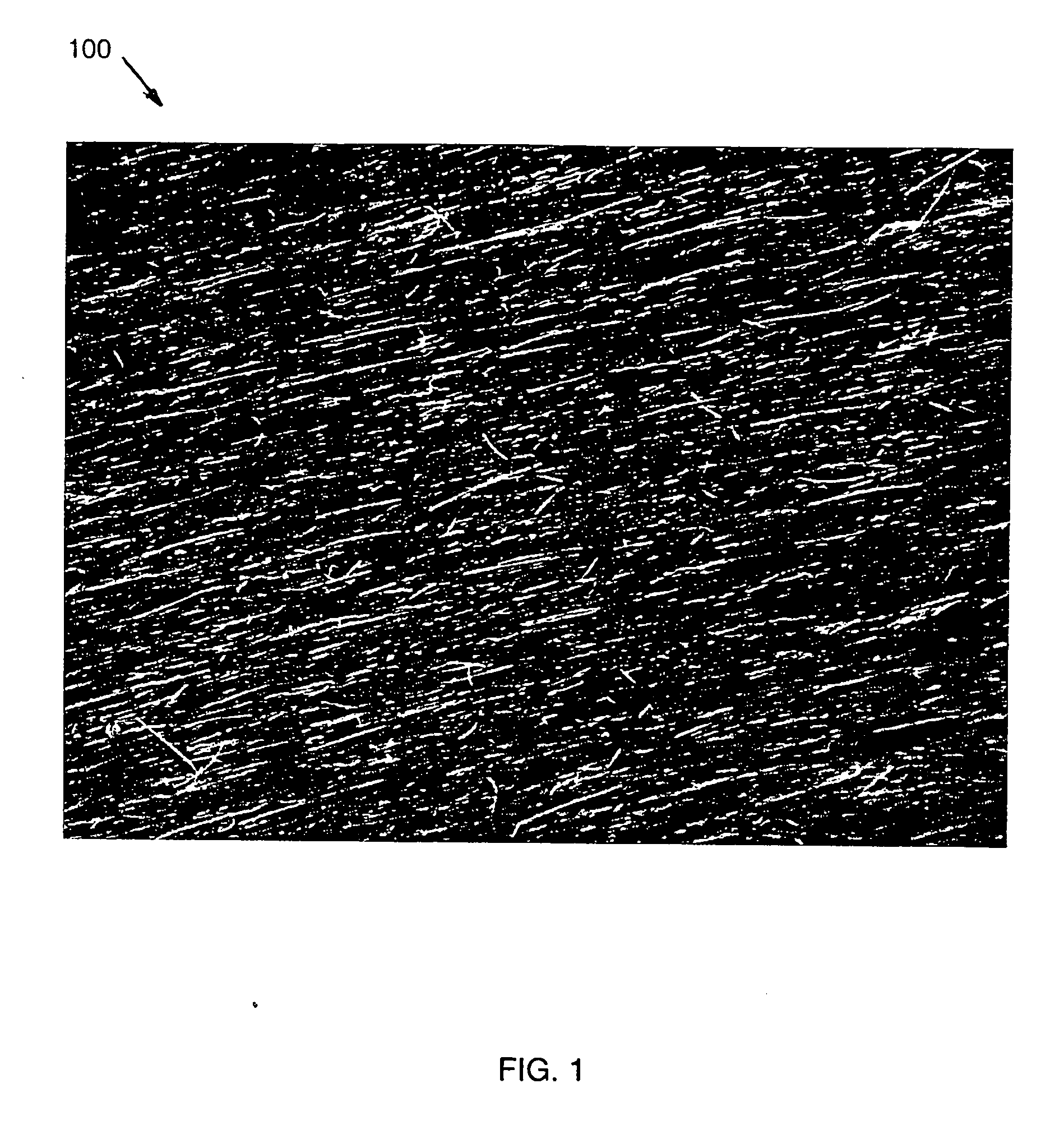
[0114] It should be appreciated that the particular implementations shown and described herein are examples of the invention and are not intended to otherwise limit the scope of the present invention in any way. Indeed, for the sake of brevity, conventional electronics, manufacturing, semiconductor devices, and nanowire (NW), nanorod, nanotube, and nanoribbon technologies and other functional aspects of the systems (and components of the individual operating components of the systems) may not be described in detail herein. Furthermore, for purposes of brevity, the invention is frequently described herein as pertaining to nanowires, and to a semiconductor transistor device. Moreover, while the number of nanowires and spacing of those nanowires are provided for the specific implementations discussed, the implementations are not intended to be limiting and a wide range of the number of nanowires and spacing can also be used. It should be appreciated that although nanowire...


PUM


Abstract

A method and apparatus for an electronic substrate having a plurality of semiconductor devices is described. A thin film of nanowires is formed on a substrate. The thin film of nanowires is formed to have a sufficient density of nanowires to achieve an operational current level. A plurality of semiconductor regions are defined in the thin film of nanowires. Contacts are formed at the semiconductor device regions to thereby provide electrical connectivity to the plurality of semiconductor devices. Furthermore, various materials for fabricating nanowires, thin films including p-doped nanowires and n-doped nanowires, nanowire heterostructures, light emitting nanowire heterostructures, flow masks for positioning nanowires on substrates, nanowire spraying techniques for depositing nanowires, techniques for reducing or eliminating phonon scattering of electrons in nanowires, and techniques for reducing surface states in nanowires are described.

Description

CROSS-REFERENCE TO RELATED APPLICATIONS [0001] This application is a continuation of U.S. patent application Ser. No. 10 / 674,060 filed Sep. 30, 2003 which claims priority to the following U.S. Provisional Applications, all of which are incorporated herein by reference in their entireties: Provisional Application No. 60 / 414,323 (Atty. Dkt. No. 2132.0010000), filed Sep. 30, 2002; Provisional Application No. 60 / 414,359 (Atty. Dkt. No. 2132.0020000), filed Sep. 30, 2002; Provisional Application No. 60 / 468,276 (Atty. Dkt. No. 2132.0150000), filed May 7, 2003; Provisional Application No. 60 / 474,065 (Atty. Dkt. No. 2132.0070001), filed May 29, 2003; and Provisional Application No. 60 / 488,801 (Atty. Dkt. No. 2132.0080000), filed Jul. 22, 2003.BACKGROUND OF THE INVENTION [0002] 1. Field of the Invention [0003] The present invention relates to semiconductor devices, and more particularly, to the use of thin films of nanowires in semiconductor devices. [0004] 2. Background Art [0005] An intere...

Claims


Application Information

Patent Timeline
IPC IPC(8): H01L21/336H01L21/38H01L29/06
CPCB82Y10/00H01F1/405H01L27/12H01L29/0665H01L29/0673H01L29/068H01L29/78696H01L31/035281H01L33/20H01L33/24H01L51/0048H01L51/0504H01L51/0545H01L51/0595H01L33/18Y10S977/742Y10S977/762Y10S977/781Y10S977/938Y10S977/789H01L27/1292H01L27/092H10K85/221H10K10/701H10K10/466H10K10/40H10K10/00
Inventor DUAN, XIANGFENGNIU, CHUNMINGEMPEDOCLES, STEPHENROMANO, LINDA T.CHEN, JIANSAHI, VIJENDRABOCK, LAWRENCESTUMBO, DAVIDPARCE, J. WALLACEGOLDMAN, JAY L.
Owner ONED MATERIAL INC
Why Eureka
Try Eureka