Method for preparing sic crystal and sic crystal

a technology of sic crystal and sic crystal, which is applied in the growth process of polycrystalline materials, crystal growth processes, chemically reactive gases, etc., can solve the problems of enlarge the device area and yield drop, and achieve the effect of increasing the number of hollow core defects

Inactive Publication Date: 2005-08-18
SHOWA DENKO KK
View PDF1 Cites 20 Cited by
  • Summary
  • Abstract
  • Description
  • Claims
  • Application Information

AI Technical Summary

Benefits of technology

[0017] The SiC single crystal film according to the present invention is a SiC single crystal film fabricated according to the above described processes, characterized in that the number of hollow-core defects that have propagated from the substrate is reduced and in that it comprises a desired film property. The SiC single crystal film encompasses both a SiC single crystal film on the substrate used in the fabrication thereof, and a S...

Problems solved by technology

When the surface area of the semiconductor device is enlarged, the probability that micropipes 101 will be contained...

Method used


Image

  • Method for preparing sic crystal and sic crystal
  • Method for preparing sic crystal and sic crystal
  • Method for preparing sic crystal and sic crystal

Examples


example 1

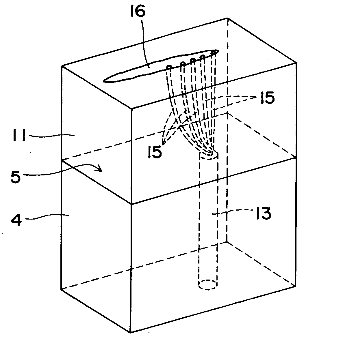
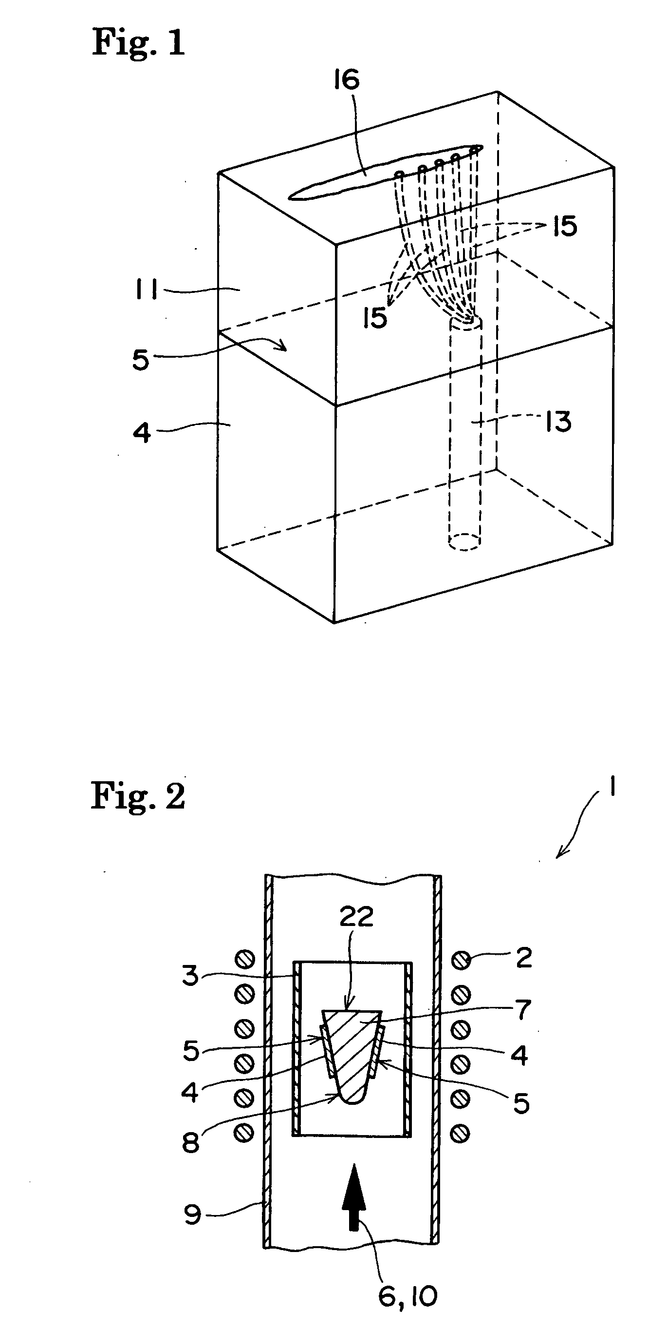
[0092] A SiC crystal 11 was fabricated by epitaxial growth using a radiant heating reactor, which is a vertical hot-wall CVD, which employed the fabrication apparatus illustrated in FIG. 2. The temperature at a top face 22 of a susceptor 7 was measured by a pyrometer via a quartz window arranged on an upper part of the reactor tube 9. This temperature measured by the pyrometer was set as the growth temperature. The growth temperatures given below are all, therefore, the measured temperatures of a top face 22 of the susceptor 7.

[0093] As the SiC single crystal substrate 4, a commercially available 8° off 4H-SiC (0001) substrate (manufactured by Cree, Inc) having a diameter of 50 mm was cut into a predetermined size (¼) for use. The SiC single crystal substrate 4 was set on the susceptor 7 in the reactor, and the remaining gases in the reactor were evacuated to create a vacuum of 10−7 Torr or below. Hydrogen gas only was then charged into the reactor, wherein the surface of the SiC s...

example 2

[0097] SiC crystals were layered under the same conditions as those in Example 1, except for the C / Si ratio of the source gas 6 being changed to be in a range from 0.4 to 1.0, wherein the nitrogen concentration, which was the impurity concentration, of the SiC crystals was measured when the C / Si ratio was changed to be in the range of from 0.4 to 1.0. The results are shown in FIG. 5. As illustrated in FIG. 5, under the above-described conditions the optimal range for the C / Si ratio in which the nitrogen concentration, as impurities, is at a minimum is from 0.8 to 0.9. When the C / Si ratio is lower than that at 0.4 to 0.7, the nitrogen concentration increases as the C / Si ratio decreases. When the C / Si ratio is higher than that at 1.0 or more, semiconductor device properties switched from being n-type to p-type. It was therefore learned that for an epilayer to be used for an n-type high-voltage device, a suitable range for the C / Si ratio was from 0.6 to 0.9 in which the formed SiC crys...

example 3

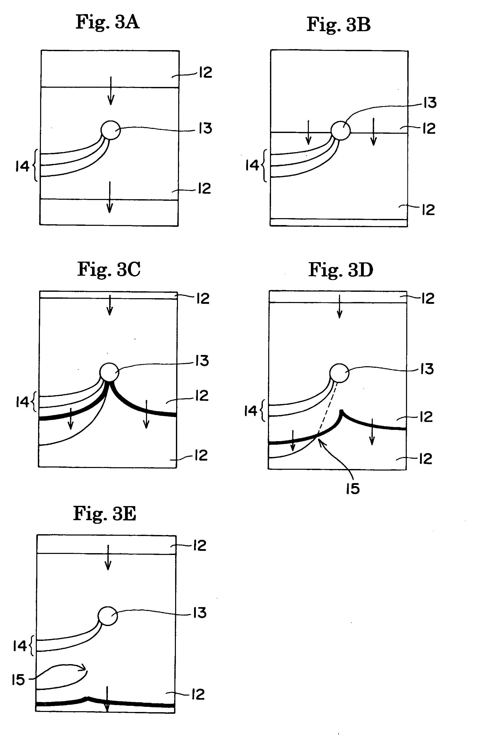
[0099] SiC crystals 11 were grown by varying the C / Si ratio from 0.6 to 0.9 while keeping the other conditions the same as in Example 1, for investigating the closing probability of micropipe 13 that existed on the SiC substrate. The results are shown in FIG. 4A. From FIG. 4A it can be seen that although the closing probability is less than 1% when the C / Si ratio was approximately 0.9, when the C / Si ratio was lowered, whereby the conditions were made to be excess in Si, the probability of micropipe closing rose, so that at 0.6 the closing probability was 99% or more.

[0100] Therefore, it is clear that with this fabrication apparatus 1 a very suitable SiC crystal 11 for use in a semiconductor device can be obtained when the C / Si ratio is 0.6, which is determined by the carbon atom supply limitation, because the closing probability reaches 99% or more, and from the results of Example 2 there are no problems with surface morphology.


PUM


Abstract

A process for closing hollow-core defects, called micropipes, during growth by CVD of a SiC crystal on a SiC single crystal substrate having hollow-core defects, and a crystal obtained according to the process, by contacting the SiC crystal with a source gas adjusted to a C/Si atom ratio range in which the crystal growth rate is determined by the carbon atom supply limitation, then epitaxially growing and laminating a plurality of SiC crystal layers, wherein hollow-core defects in the SiC single crystal substrate dissociate into a plurality of dislocations given by small Burgers vector in order not to propagate to the crystal surface. In addition, the present invention provides a fabrication process of a SiC crystal, wherein a first SiC crystal is made as a buffer layer, and a further SiC crystal is layered thereon using a source gas adjusted to be higher than that of the C/Si ratio when forming the buffer layer, whereby a desired film property is conferred.

Description

TECHNICAL FIELD [0001] The present invention relates to a fabrication process of a SiC crystal having a reduced number of hollow-core defects, which are called micropipes, in the SiC substrate. The present invention further relates to the SiC crystal and a SiC single crystal film obtained from such a fabrication process, a SiC semiconductor device and a SiC single crystal substrate comprising such a SiC single crystal film, an electronic device using such a SiC single crystal substrate, and a fabrication process of a SiC bulk crystal which uses the above described SiC crystal as a seed crystal. BACKGROUND ART [0002] Research has been progressing into silicon carbide SiC as a semiconductor device for high performance power devices or as a substrate for devices having high voltage, low-loss and which are operable at high temperatures in view of silicon carbide SiC's excellent physical properties of wide bandgap, a high reverse blocking voltage and high thermal conductivity. [0003] To ...

Claims


Application Information

Patent Timeline
IPC IPC(8): C30B25/02
CPCC30B25/02C30B29/36
Inventor KAMATA, ISAHOTSUCHIDA, HIDEKAZU
Owner SHOWA DENKO KK
Why Eureka
Try Eureka