Three-dimensional quantum dot structure for infrared photodetection

a quantum dot and optical path technology, applied in the field of three-dimensional quantum dot optical path structure, can solve the problems of inability to accurately detect the location of quantum dots, and inability to produce thin sige film thicknesses, etc., to achieve improved spectral sensitivity and reproducibility, and the effect of precise location and distribution of quantum dots

Active Publication Date: 2005-09-08
MICROSOFT TECH LICENSING LLC
View PDF12 Cites 25 Cited by
  • Summary
  • Abstract
  • Description
  • Claims
  • Application Information

AI Technical Summary

Benefits of technology

[0018] The present invention is a three-dimensional quantum dot structure formed from a simple one-layer deposition, using surface relief aspects of the substrate. With a pre-arranged substrate orientation, the precise location of quantum dots, as well as their size and distribution, can be reliably controlled. Therefore, an IR detector of improved spectral sensitivity and reproducibility can be fabricated.

Problems solved by technology

While a thick SiGe is desirable for light absorption, too thick of a SiGe film causes a defect generation that is responsible for dark currents.
Higher Ge concentrations and higher device process temperatures result in the formation of thinner SiGe film thicknesses.
Once the SiGe thickness is grown beyond its critical thickness, lattice defects in SiGe are inevitable.
As mentioned above, an IR photo detector built from a SiGe film with lattice defects generates large dark currents and noise.
The absorption coefficient of any SiGe alloy is relatively small and the limited thickness dictated by the critical thickness further limits the ability of SiGe films to absorb photons.
However, this optical path design necessarily limits the design of IR detectors.
However, it is very difficult to grow a defect-free thick SiGe film on a Si substrate because of the lattice mismatch between these two materials.
However, growing the SiGe by a blanket deposition technique results in SiGe growth on the bottom of the trenches and top of the wafer, as well as on the sidewalls.
However, this approach is expensive and difficult.
But QWIPs are insensitive to normal incident light.
However, these 2D quantum dot processes are relatively complex.

Method used


Image

  • Three-dimensional quantum dot structure for infrared photodetection
  • Three-dimensional quantum dot structure for infrared photodetection
  • Three-dimensional quantum dot structure for infrared photodetection

Examples


Embodiment Construction

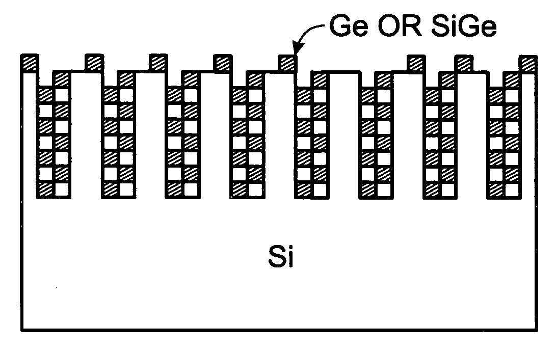
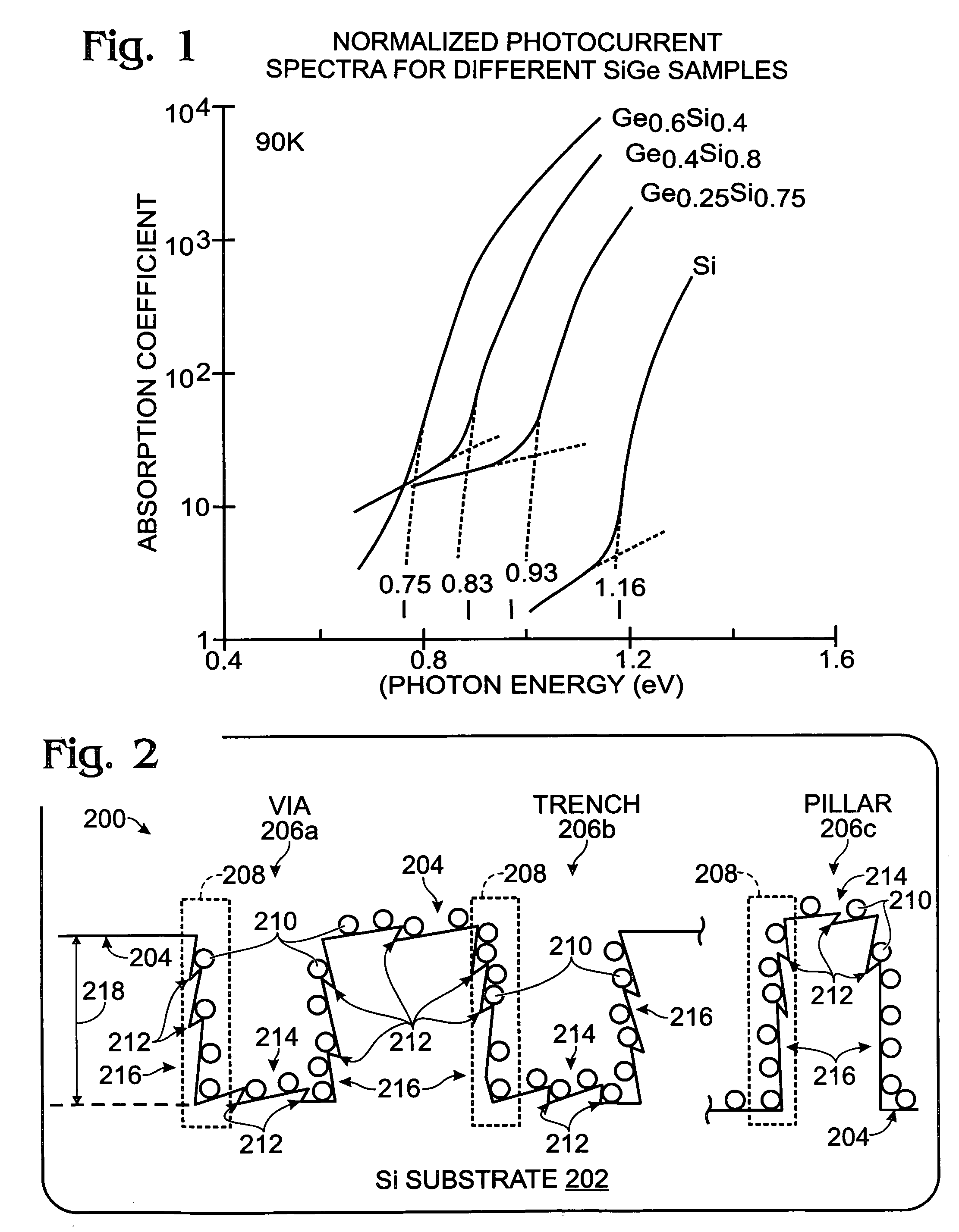
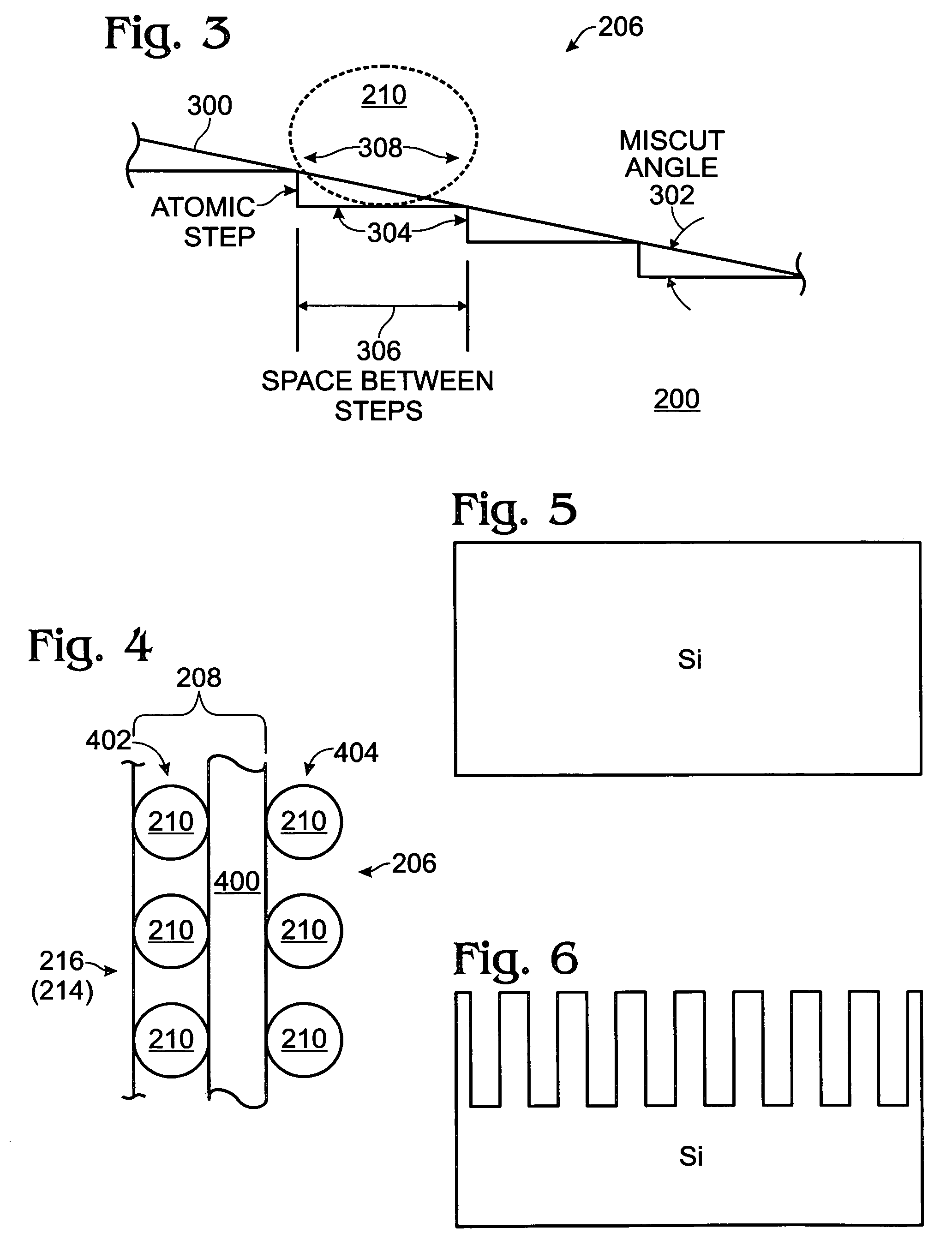
[0029]FIG. 2 is a partial cross-sectional view of the present invention 3D quantum dot optical path structure for IR photodetection. The structure 200 comprises a single-crystal Si substrate 202 with a surface 204. A Si feature 206 is formed in the Si substrate surface 204. More specifically, a via feature 206a, trench feature 206b, and pillar feature 206c are shown. A 3D optical path 208 with dots 210 of a first material including germanium (Ge) is formed on Si feature.

[0030] The optical path first material dots 210 include a first material of either Ge or SiGe. Alternately stated, the dots have a Ge concentration in the range from 5 to 100%. In one aspect of the structure 200, the Si feature 206 includes defect sites 212. The dots 210 are more likely to form in the defect sites than on the feature sidewalls 216 or feature surfaces 214. The Si feature 206 has a height 218 that is in the range of 0.3 to 5 microns. In other aspects of the invention, the substrate 200 need not single...


PUM


Abstract

A 3D quantum dot optical path structure is provided, along with a method for selectively forming a 3D quantum dot optical path. The method comprises: forming a single crystal Si substrate with a surface; forming a Si feature in the substrate, such as a via, trench, or pillar; forming dots from a Ge or SiGe material overlying the Si feature; and, forming an optical path that includes the dots. In some aspects of the method, the Si feature has defect sites. For example, the Si feature may be formed with a miscut angle. As a result of the miscut angle, steps are formed in the Si feature plane. Then, the dots are formed in the Si feature steps. The miscut angle is in the range between 0.1 and 5 degrees, and the spacing between steps is in the range between 1 and 250 nanometers (nm).

Description

RELATED APPLICATIONS [0001] This application is a continuation-in-part of a pending patent application entitled, SURFACE-NORMAL OPTICAL PATH STRUCTURE FOR INFRARED PHOTODETECTION, invented by Lee et al., Ser. No. ______, filed ______, attorney docket no. SLA826. [0002] This application is a continuation-in-part of a pending patent application entitled, VERTICAL OPTICAL PATH STRUCTURE FOR INFRARED PHOTODETECTION, invented by Tweet et al., Ser. No. ______, filed ______, attorney docket no. SLA831.BACKGROUND OF THE INVENTION [0003] 1. Field of the Invention [0004] This invention generally relates to integrated circuit (IC) fabrication processes and, more particularly, to a quantum dot three-dimensional optical path structure and corresponding fabrication method. [0005] 2. Description of the Related Art [0006] There are many applications for photodetection in the near infrared region (the wavelength between 0.7 micron to 2 microns), such as in fiber-optical communication, security, and ...

Claims


Application Information

Patent Timeline
Patent Type & Authority Applications(United States)
IPC IPC(8): H01L21/00H01L21/66H01L31/0352
CPCB82Y10/00H01L31/035236B82Y20/00
Inventor MAA, JER-SHENLEE, JONG-JANTWEET, DOUGLAS J.HSU, SHENG TENG
Owner MICROSOFT TECH LICENSING LLC
Why Eureka
Try Eureka