Semiconductor device and method for fabricating the same

a semiconductor and device technology, applied in the direction of semiconductor lasers, polycrystalline material growth, crystal growth process, etc., can solve the problems of difficult cleavage of the entire substrate, difficult cleavage, and prevented the formation of satisfactory resonator surfaces

Inactive Publication Date: 2005-09-15
PANASONIC CORP
View PDF6 Cites 20 Cited by
  • Summary
  • Abstract
  • Description
  • Claims
  • Application Information

AI Technical Summary

Benefits of technology

[0013] It is therefore an object of the present invention to provide a method for fabricating a semiconductor device having a very thin epitaxially grown laser separated from the substrate for the epitaxial growth containing a reduced number of crystal defects.

Problems solved by technology

However, it has been difficult to cleave the entire substrate since the crystal structure of the sapphire substrate has rotated by 30° from that of the nitride semiconductor in the c plane ((0001) surface)) and sapphire is hard to be cleaved.
This has prevented the formation of satisfactory resonator surfaces (mirrors) and made it difficult to achieve a high performance semiconductor laser, especially with a low threshold current.
However, the foregoing method for fabricating a nitride semiconductor device has the following problems.
If the nitride semiconductor layers on the sapphire substrate are increased in film thickness, however, the bowing of the entire wafer during cooling after epitaxial growth becomes conspicuous due to the different thermal expansion coefficients of the sapphire substrate and the nitride semiconductor layers so that it is difficult to adhere the flat recipient substrate to the wafer.

Method used


Image

  • Semiconductor device and method for fabricating the same
  • Semiconductor device and method for fabricating the same
  • Semiconductor device and method for fabricating the same

Examples


embodiment 1

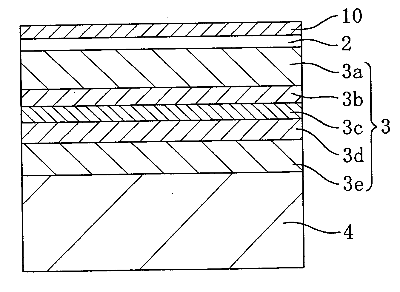
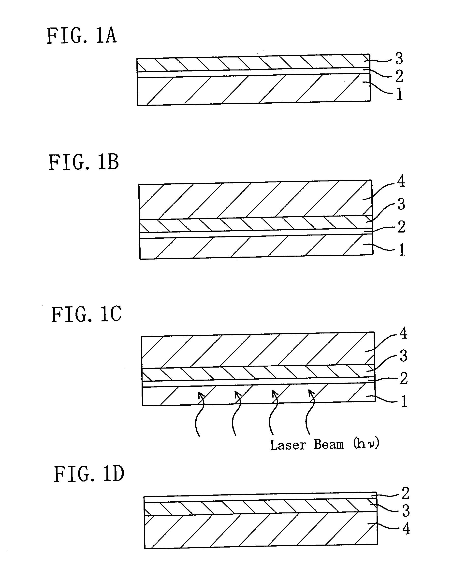
[0071]FIGS. 1A to 1D are cross-sectional views illustrating a method for fabricating a semiconductor device according to a first embodiment of the present invention. First, in the step shown in FIG. 1A, a sapphire substrate 1 (wafer) having a principal surface substantially coincident with the (0001) plane (c plane) is prepared. Then, a ZnO layer 2 having a thickness of about 100 nm and serving as a spacer layer is formed by, e.g., RF sputtering on the sapphire substrate 1. Subsequently, an epitaxially grown layer 3 (with a thickness of 5 μm) having a multilayer structure including a GaN layer, an AlGaN layer, and an InGaN layer, each of which is of p-type, of n-type, or undoped, is formed on the ZnO layer 2 by metal organic chemical vapor deposition (MOCVD). In the case of fabricating a semiconductor laser, a waveguide structure has been incorporated into the epitaxially grown layer 3 by using a regrowth technique, selective etching or the like.

[0072] Next, in the step shown in FI...

embodiment 2

[0082]FIGS. 5A to 5D are cross-sectional views illustrating a method for fabricating a semiconductor device according to a second embodiment of the present invention.

[0083] First, in the step shown in FIG. 5A, a sapphire substrate 1 (wafer) having a principal surface substantially coincident with the (0001) plane (c plane) is prepared. Then, an In0.1Ga0.09N layer 5 having a thickness of about 30 nm and serving as a spacer layer is formed by, e.g., MOCVD on the sapphire substrate 1. Subsequently, an epitaxially grown layer 3 (with a thickness of 5 μm) having a multilayer structure including a GaN layer, an AlGaN layer, and an InGaN layer, each of which is of p-type, of n-type, or undoped, is formed on the In0.1Ga0.9N layer 5 by MOCVD performed in the same apparatus. In the case of fabricating a semiconductor laser, a waveguide structure has been incorporated into the epitaxial layer 3 by using a regrowth technique, selective etching or the like.

[0084] Next, in the step shown in FIG...

embodiment 3

[0092]FIGS. 7A to 7D are cross-sectional views illustrating a method for fabricating a semiconductor device according to a third embodiment of the present invention.

[0093] First, in the step shown in FIG. 7A, a sapphire substrate 1 (wafer) having a principal surface substantially coincident with the (0001) plane (c plane) is prepared. Then, an In0.1Ga0.9N layer 5 having a thickness of about 30 nm and serving as a spacer layer is formed by, e.g., MOCVD on the sapphire substrate 1. Subsequently, an epitaxially grown layer 3 (with a thickness of 5 μm) having a multilayer structure including a GaN layer, an AlGaN layer, and an InGaN layer, each of which is of p-type, of n-type, or undoped, is formed on the In0.1Ga0.9N layer 5 by MOCVD performed in the same apparatus. In the present embodiment, an Al0.1Ga0.9N layer is formed in direct contact with the In0.1Ga0.9N layer 5. In the case of fabricating a semiconductor laser, a waveguide structure has been incorporated into the epitaxial lay...


PUM


Abstract

A spacer layer is formed on a single-crystal substrate and an epitaxially grown layer composed of a group III-V compound semiconductor layer containing a nitride or the like is further formed on the spacer layer. The epitaxially grown layer is adhered to a recipient substrate. The back surface of the single-crystal substrate is irradiated with a light beam such as a laser beam or a bright line spectrum from a mercury vapor lamp such that the epitaxially grown layer and the single-crystal substrate are separated from each other. Since the forbidden band of the spacer layer is smaller than that of the single-crystal substrate, it is possible to separate the thin semiconductor layer from the substrate by decomposing or fusing the spacer layer, while suppressing the occurrence of a crystal defect or a crack in the epitaxially grown layer.

Description

BACKGROUND OF THE INVENTION [0001] The present invention relates to a method for fabricating a semiconductor device for use as, e.g., a short-wavelength light-emitting diode, a short-wavelength semiconductor laser, or a high-temperature and high-speed transistor. [0002] A nitride semiconductor which has a large optical band gap (e.g., GaN has an optical band gap of about 3.4 eV at a room temperature) has been conventionally used as a material for implementing a visible light-emitting diode which emits light in a relatively short wavelength region such as green, blue, or white light or a short-wavelength semiconductor laser which would be used for future high density optical disks. In particular, a nitride semiconductor has been used prevalently for the active layer of a light-emitting diode. As a light source for a read / write operation to a high-density optical disk, the commercialization of a blue or blue-purple laser has been in strong demand. [0003] It is general practice to form...

Claims


Application Information

Patent Timeline
Patent Type & Authority Applications(United States)
IPC IPC(8): H01L21/268H01L29/20H01L33/06H01L33/12H01L33/16H01L33/28H01L33/32H01L33/34H01L33/44H01S5/02H01S5/323H01S5/343
CPCB82Y20/00H01S2301/173C30B29/40C30B29/403C30B29/406H01L21/0242H01L21/02458H01L21/02472H01L21/0254H01L21/268H01L29/2003H01L33/025H01L33/06H01S5/0213H01S5/0215H01S5/0217H01S5/0218H01S5/3202H01S5/34333C30B25/183H01S5/320225H01S5/0202
Inventor UEDA, TETSUZO
Owner PANASONIC CORP
Why Eureka
Try Eureka