Image sensor comprising isolated germanium photodetectors integrated with a silicon substrate and silicon circuitry

a germanium photodetector and image sensor technology, applied in the direction of interferometer, radio frequency control device, instruments, etc., can solve the problems of bonding process reliability, size and speed, bonding failure, etc., and achieve the effect of reducing signal degradation

Active Publication Date: 2005-09-22
INFRARED NEWCO
View PDF61 Cites 76 Cited by
  • Summary
  • Abstract
  • Description
  • Claims
  • Application Information

AI Technical Summary

Benefits of technology

[0014] At each picture element, or pixel, the germanium element converts the incoming illumination into an electrical signal. Silicon circuitry at the pixel detects and amplifies the signal from the germanium element. The pixels are read, as by row and column addressing circuitry, to read out and uniquely identify the output of each pixel. Thus an image is read out from the array. Since germanium is photosensitive from the visible through the infrared up to wavelengths of about 1.7 μm, both visible and infrared images may be formed. The signal from each pixel is converted from an analog current or voltage to a digital value before being transmitted off-chip. This minimizes signal degradation. In a preferred embodiment, each germanium pixel is epitaxially grown on the silicon as a small crystalline island in a dielectric surface cladding.

Problems solved by technology

Unfortunately, the process technology for the newer detector materials is incompatible with the technology to process the silicon readout electronics.
While the indium bump bonding process has enabled new applications at higher temperatures, the bonding process presents problems with reliability, processing, size and speed.
Thermal expansion mismatch, high g forces, and vibration all can cause the bonds to fail.
Thermal mismatch between the detector material and the silicon ROIC is a particular problem because cooling of the image sensor is required for many applications to reduce the detector dark current.
Barton [2] teaches a method employing a third substrate material to lessen the thermal mismatch problem, but the third material adds complexity and increases cost.
High g forces that can cause bump bonding failures are often encountered by image sensor devices employed in space applications, and in all applications moderate vibration of the hybridized image sensor can cause individual detectors (pixels) to fail.
These limitations are extremely detrimental given the harsh field environments these devices are likely to experience.
The added steps of bonding also increase cost and reduce yield.
Thinned arrays are difficult to handle during assembly, and this difficulty adds to the yield problems accompanying indium bump bonding.
Indium bump bonds also limit reduction in the size of individual pixels.
Since larger array size limits the image resolution, and larger FPA dimensions increase the size of the optics required to fully illuminate the array, bump bonding is disadvantageous in applications where camera weight and volume are critical.
Indium bump bonds further limit the speed of image sensors needed for applications such as 3-D LADAR imaging.
Indium bump bonds present an additional capacitive load that slows down the detection and readout electronics.
In addition, the bonds increase the power consumption and increase the pixel-to-pixel capacitance thereby increasing the array noise and complicating noise analysis [4].

Method used


Image

  • Image sensor comprising isolated germanium photodetectors integrated with a silicon substrate and silicon circuitry
  • Image sensor comprising isolated germanium photodetectors integrated with a silicon substrate and silicon circuitry
  • Image sensor comprising isolated germanium photodetectors integrated with a silicon substrate and silicon circuitry

Examples


Embodiment Construction

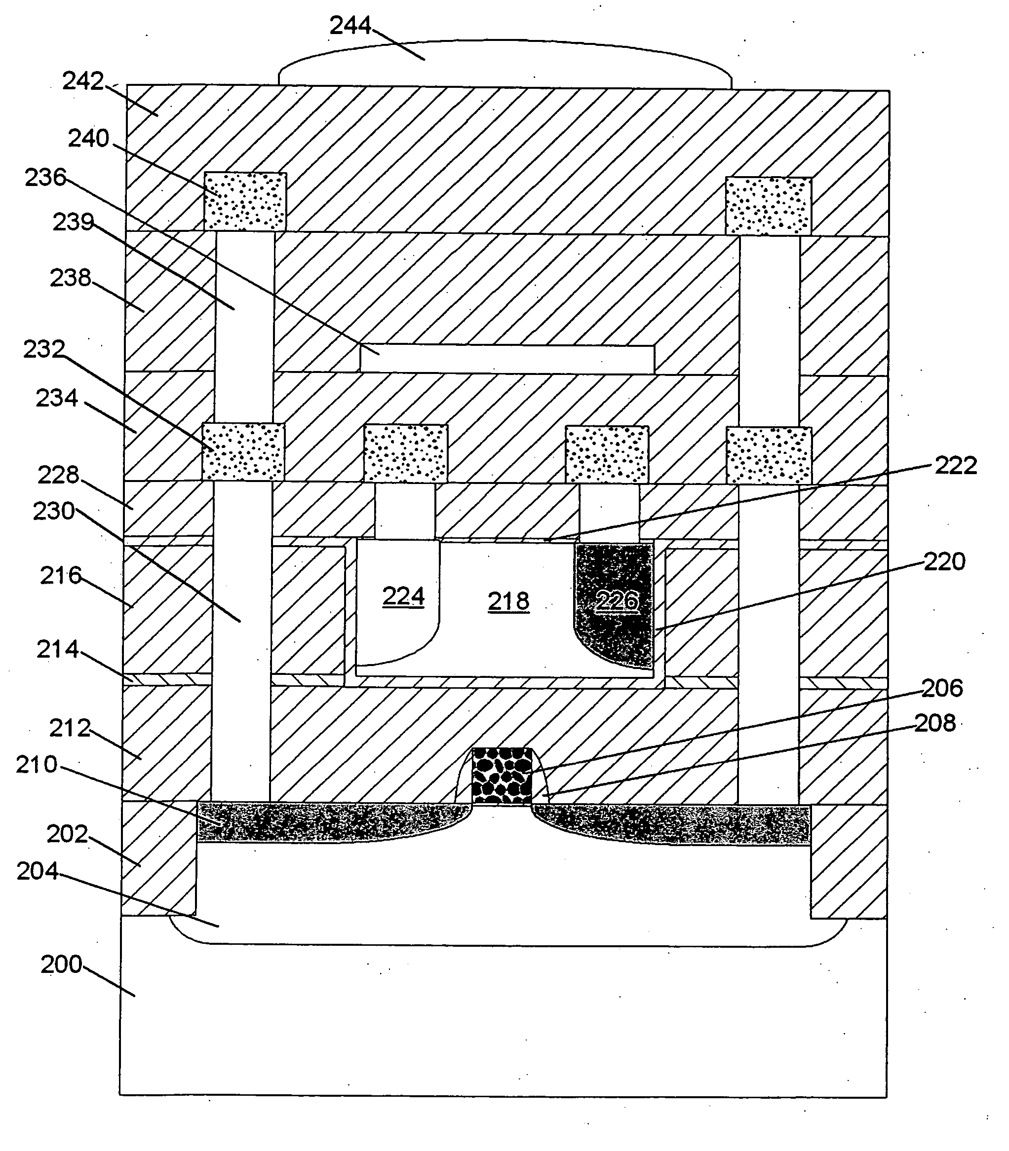
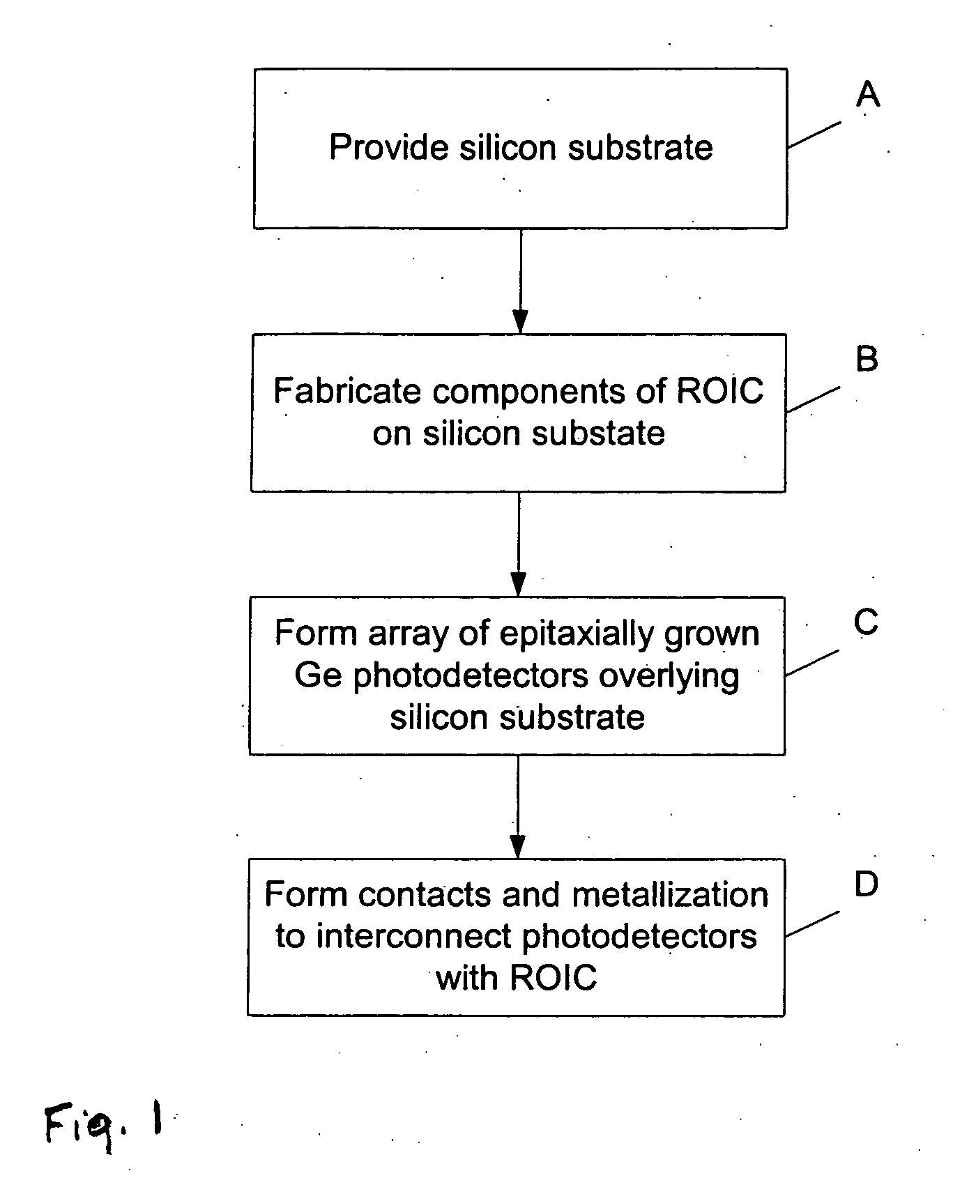
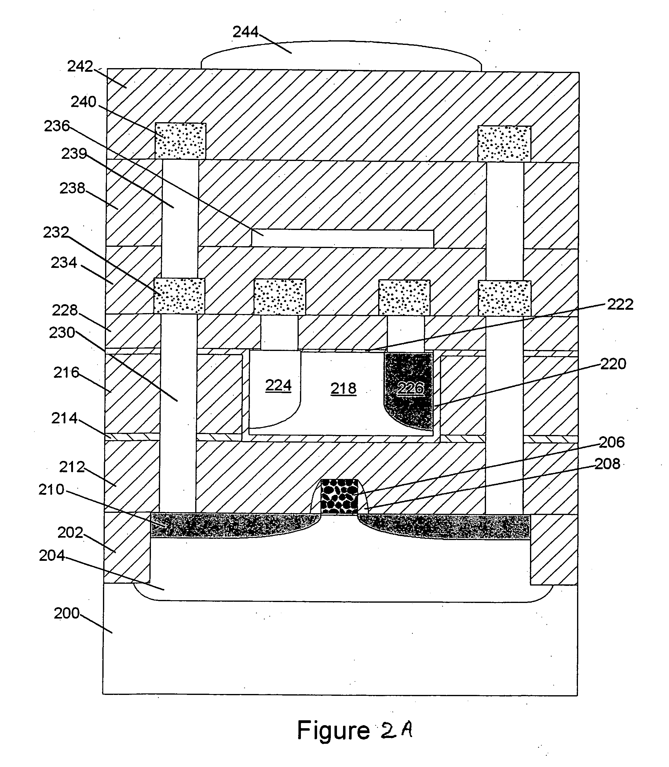
[0025] Referring to the drawings, FIG. 1 is a schematic flow diagram of a preferred method of fabricating an image sensor. The method will also be described by reference to FIGS. 2A and 2B. FIG. 2A displays the final device structure through metallization and the inclusion of a microlens on each pixel, and FIG. 2B displays the cross section of the device including a Ge seed layer.

[0026] As shown in Block A of FIG. 1, the first step in the fabrication process is to provide a substrate comprising silicon. The silicon is selected or chosen to have the resistivity and crystal orientation appropriate for the chosen silicon device processing technology, usually CMOS or BiCMOS processing.

[0027] The next step (Block B) is to fabricate components of the silicon readout integrated circuitry (ROIC) in the silicon substrate in accordance with the chosen silicon processing technique.

[0028] Referring to FIG. 2A, an exemplary fabrication begins with a silicon substrate 200. A shallow trench iso...


PUM


Abstract

In accordance with the invention, an improved image sensor comprises an array of germanium photosensitive elements integrated with a silicon substrate and integrated with silicon readout circuits. The silicon transistors are formed first on a silicon substrate, using well known silicon wafer fabrication techniques. The germanium elements are subsequently formed overlying the silicon by epitaxial growth. The germanium elements are advantageously grown within surface openings of a dielectric cladding. Wafer fabrication techniques are applied to the elements to form isolated germanium photodiodes. Since temperatures needed for germanium processing are lower than those for silicon processing, the formation of the germanium devices need not affect the previously formed silicon devices. Insulating and metallic layers are then deposited and patterned to interconnect the silicon devices and to connect the germanium devices to the silicon circuits. The germanium elements are thus integrated to the silicon by epitaxial growth and integrated to the silicon circuitry by common metal layers.

Description

CROSS REFERENCES TO RELATED APPLICATIONS [0001] This application claims the benefit of U.S. Provisional Application Ser. No. 60 / 510,932 filed by C. A. King and C. S. Rafferty on Oct. 13, 2003 entitled “Method to Fabricate an Integrated Image Sensor Using Isolated Germanium Photodetectors”, which application is incorporated herein by reference. [0002] This application is also a continuation-in-part of U.S. patent application Ser. No. 10 / 453,037 filed by J. Bude, et al. on Jun. 3, 2003 and entitled “Semiconductor Devices With Reduced Active Region Defects and Unique Contacting Schemes.” The '037 application, in turn, claims the benefit of U.S. Provisional Application Ser. No. 60 / 434,359 filed Dec. 18, 2002. The foregoing application Ser. No. 10 / 453,037 and 60 / 434,359 are incorporated herein by reference.FIELD OF THE INVENTION [0003] This invention relates to image sensing devices and, in particular, to an image sensing device comprising an array of germanium photodetectors integrated ...

Claims


Application Information

Patent Timeline
Patent Type & Authority Applications(United States)
IPC IPC(8): H01L27/14H01L27/146H01L31/00
CPCH01L27/14632H01L27/14643H01L27/14649H01L21/02639H01L21/02381H01L21/02532H01L27/14634H01L2924/351H01L31/028
Inventor KING, CLIFFORD ALANRAFFERTY, CONOR S.
Owner INFRARED NEWCO
Why Eureka
Try Eureka