Organic electroluminescence display apparatus

a display apparatus and electroluminescence technology, applied in the direction of discharge tube luminescnet screens, discharge tube/lamp details, electric discharge lamps, etc., can solve the problems of high upper electrode resistance, difficult fabrication of mask sheets for large-size products, and high resistance of top electrodes, so as to prevent uniform distribution of emitted light brightness, reduce voltage drop, and reduce aperture ratio

Active Publication Date: 2005-09-29
SAMSUNG DISPLAY CO LTD +1
View PDF2 Cites 90 Cited by
  • Summary
  • Abstract
  • Description
  • Claims
  • Application Information

AI Technical Summary

Benefits of technology

[0033] As discussed above, the present invention can reduce voltage drop at a pixel far removed from a power supply point and prevent ununiform distribution of emitted light brightness in the display region even in a large-size, organic EL display apparatus of top emission structure. At the same time, it is free of a problem of reduced aperture ratio, because a member functioning as an auxiliary electrode is an electroconductive shadow pattern, which is connected to an upper electrode at a point immediately below the pattern. Adoption of a top emission structure extends element service life, because it works at a lower light intensity per unit area than a bottom emission structure for securing the same brightness.
[0034] Moreover, the organic light-emitting layer producing the above effects can be formed by vapor deposition with a mask having apertures provided over the entire display region instead of a mask having precisely fabricated apertures for each pixel. This reduces production cost and lead time from those required by vapor deposition with a mask having precisely fabricated apertures for each pixel.

Problems solved by technology

A top emission structure involves problems, when it is applied to large-size, organic EL display apparatuses.
Thus, the problems result from high upper electrode resistance.
The mask sheet is difficult to fabricate for large-size products, irrespective of fabrication method, although not difficult for products of small size, low resolution and low aperture ratio.
The difficulty increases as required resolution or aperture ratio increases.

Method used


Image

  • Organic electroluminescence display apparatus
  • Organic electroluminescence display apparatus
  • Organic electroluminescence display apparatus

Examples


example 1

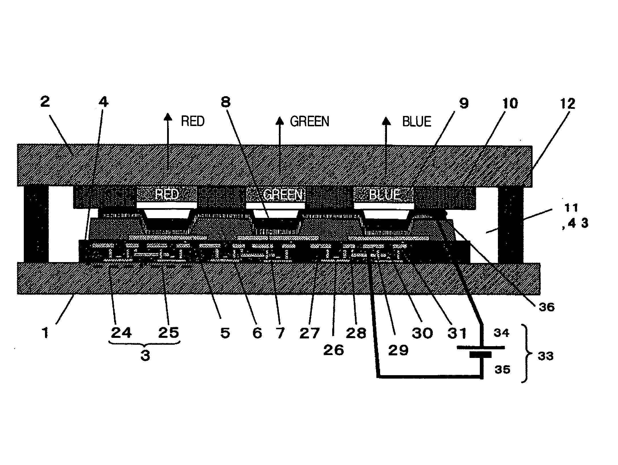
[0053] The embodiment 1 of the organic EL display apparatus of the present invention is described by referring to the drawings. FIG. 1 is a cross-sectional view illustrating the organic EL display apparatus of the embodiment 1 of the present invention.

[0054] The organic light-emitting element formed on the first substrate 1 is composed of the organic light-emitting layer 7 and upper electrode (transparent electrode) 8 on the substrate 1, the layer 7 being composed of the lower electrode 5, first injection layer, first transport layer, light-emitting layer, second transport layer and second injection layer.

[0055] Broadly speaking, the organic light-emitting element structurally falls into one of the following types.

[0056] The first type uses the lower electrode 5 as the anode and upper transparent electrode 8 as the cathode. In this case, the first injection layer and first transport layer in the organic light-emitting element 7 work as the hole injection layer and hole transport ...

example 2

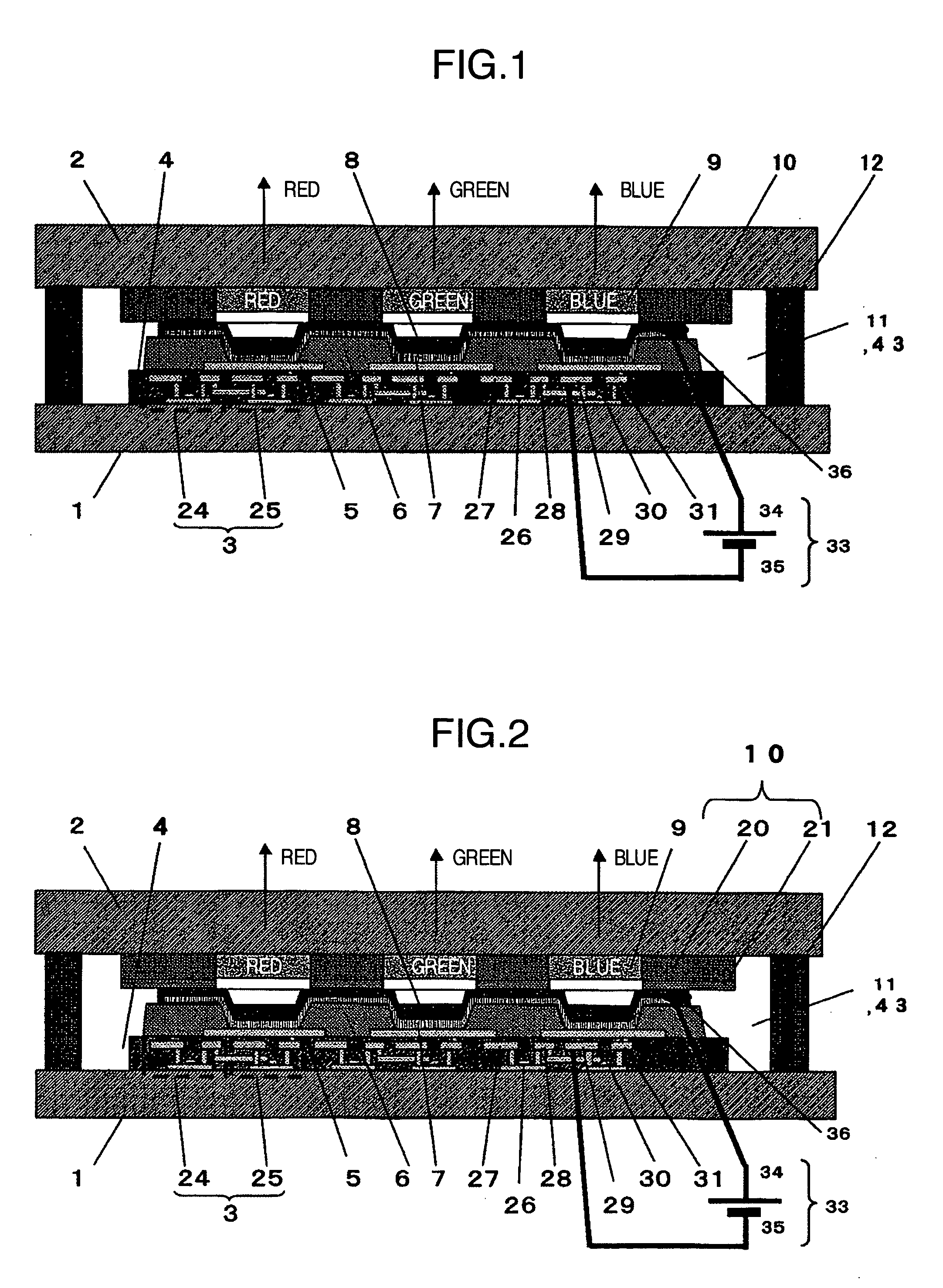
[0114]FIG. 2 is a cross-sectional view illustrating the organic EL display apparatus with an electroconductive shadow pattern of another embodiment. The electroconductive shadow pattern 10 may be of a 2-layer structure of the shadow layer 20 and electroconductive layer 21 of low resistance, as illustrated in FIG. 2. The electroconductive layer 20 can give a higher image contrast than the layer of metallic material alone, when incorporated with a black pigment. The electroconductive layer 20 may not be necessarily electroconductive. For example, the shadow layer 20 may be formed by a photo-litho process using a photosensitive polyimide dispersed with a black pigment, e.g., carbon. Moreover, it may be formed by printing depending on a line width of the shadow layer 20.

[0115] The electroconductive layer 21 of low resistance is made of a material similar to that used for the shadow pattern of the embodiment 1. The 300 nm thick upper transparent electrode 8 of ITO is formed on the first...

example 3

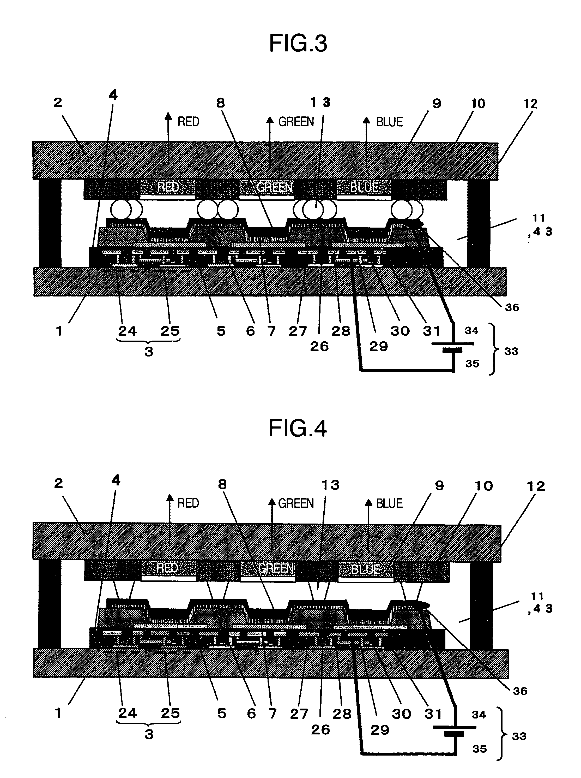
[0118]FIG. 3 is a cross-sectional view illustrating the organic EL display apparatus with spherical spacers. The substrates 1 and 2 are formed by a film-making method similar to that for EXAMPLE 1. An electroconductive polymer dispersed with gold-plated silica beads or metallic balls as the spherical spacer 13 is spread over the second substrate 2 by spin coating for a photo-litho process. This sets the spherical spacers 11 selectively on the electroconductive shadow pattern 10, as shown in FIG. 8 which presents the plan view. A spacer diameter of around 5 to 30 μm will be adequate. Then, the adhesive layer 12 is spread between the substrates 1 and 2 in a ring, and is cured with ultraviolet ray while these substrates are pressed to each other, to produce the organic EL display apparatus.


PUM


Abstract

The organic electroluminescence display apparatus of the present invention comprises a first and second substrates, the former being coated with banks for separating pixels, a lower electrode, organic light-emitting layer and upper electrode of a transparent material in this order, and the latter being coated with a color filter and electroconductive shadow pattern, wherein the organic light-emitting layer surrounded by the banks for separating pixels faces the color filter, and the first and second substrates face each other in such a way that the upper electrode over the banks for separating pixels is electrically connected to the electroconductive shadow pattern. This structure connects at least one of the upper electrode and electroconductive shadow pattern to a power supply point, to control ununiform emitted light brightness which may result from voltage drop at the upper transparent electrode. Moreover, the organic light-emitting layer can be formed without a vapor deposition mask having a precise aperture pattern, to efficiently produce the organic EL display apparatus.

Description

BACKGROUND OF THE INVENTION [0001] The present invention relates to an organic electroluminescence display apparatus. [0002] An organic electroluminescence (hereinafter referred to as “organic EL”) display apparatus is formed by arranging a plurality of elements, each being essentially of 3-layer structure with an organic light-emitting layer placed between an anode and cathode electrodes, the former for injecting holes and the latter for injecting electrons into the intermediate layer. [0003] The organic light-emitting layer is of (1) 2-layer structure with an emitting layer and hole transport layer in this order from the cathode electrode side, (2) 2-layer structure with an electron transport layer and emitting layer in this order from the cathode electrode side, or (3) 3-layer structure with an electron transport layer, emitting layer and hole transport layer in this order from the cathode electrode side. When a voltage of several volts is applied to the element between the elect...

Claims


Application Information

Patent Timeline
Patent Type & Authority Applications(United States)
IPC IPC(8): H01J1/62H05B33/26H01L27/32H01L51/50H01L51/52H05B33/04H05B33/06H05B33/12H05B33/14H05B33/22
CPCH01L27/322H01L27/3246H01L51/5237H01L51/5206H01L27/3276H10K59/38H10K59/122H10K59/131H10K50/814H10K50/824H10K50/8428H10K50/846H10K50/865H10K2102/321H10K2102/3026H10K50/844
Inventor MATSUURA, HIROYASUISHIHARA, SHINGOTAKANOSU, KEIJIMATSUZAKI, EIJI
Owner SAMSUNG DISPLAY CO LTD
Why Eureka
Try Eureka