Tunnel magnetoresistance device

a tunnel barrier layer and magnetoresistance technology, applied in the manufacture of flux-sensitive heads, instruments, record information storage, etc., can solve the problems of local electric field concentration, inconvenient use, and inability to meet the needs of the user

Inactive Publication Date: 2005-10-13
DENSO CORP
View PDF11 Cites 10 Cited by
  • Summary
  • Abstract
  • Description
  • Claims
  • Application Information

AI Technical Summary

Benefits of technology

[0030] The tunnel barrier layer having substantially a stoichiometric composition has good drapability over the pinned layer. Accordingly, the thickness nonuniformity of the tunnel barrier layer is very small even if it is formed thinly on the surface of the pinned layer having large surface irregularities. Hence, the TMR device according to the invention exhibits a large MR ratio because of the small thickness of the tunnel barrier layer, and also exhibits a stable tunneling current and a small leak current because of the small thickness-nonuniformity of the tunnel barrier layer.
[0031] In addition, it is also possible to make the tunneling current more larger by utilizing the surface irregularities of the pinned layer. This is based on the fact that the effective surface area of the pinned layer increases as the surface roughness of the pinned layer increases. By utilizing the surface irregularities of the pinned layer, it becomes possible to make the surface area of the TMR device smaller.
[0041] the load lock chamber allowing the substrate to be transported from the first process chamber to the second process chamber while preventing the substrate from being exposed to an oxidation atmosphere.

Problems solved by technology

However, there is a problem in that the conventional tunnel barrier layer formed by PVD method lacks uniformity in layer thickness and layer quality.
For such reason, the thickness of the tunnel barrier layer formed by PVD method is not uniform even if the formed tunnel barrier layer is subjected to oxidizing processing.
This may cause local electric field concentration, a leak current, tunneling current variation, and pinholes within the tunnel barrier layer.
These significantly degrade the performance of the TMR device.
However, in this case, it is very difficult to control surface roughness of the pinned layer, because the pinned layer is formed by a process including the step of forming a thin metal film.
However, it is difficult to carry out such measures from economical and technical standpoints.
Such a surface phase makes it difficult to control the layer thickness of the tunnel barrier layer.
However, if the surface asperities of the pinned layer are made larger, the drapability of the tunnel barrier layer over the pinned layer becomes worse, and accordingly the performance of the TMR device is worsened.

Method used


Image

  • Tunnel magnetoresistance device
  • Tunnel magnetoresistance device
  • Tunnel magnetoresistance device

Examples


Embodiment Construction

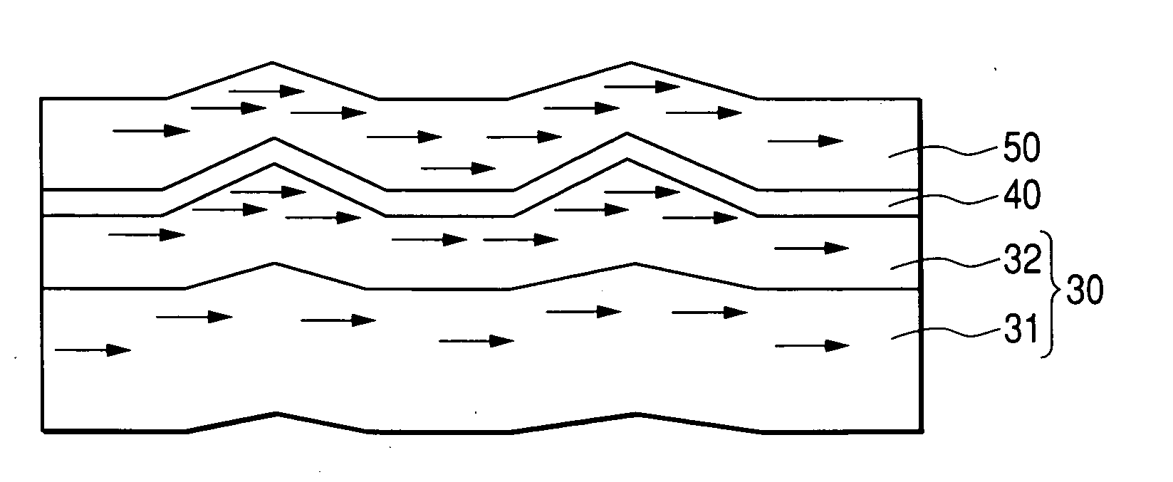
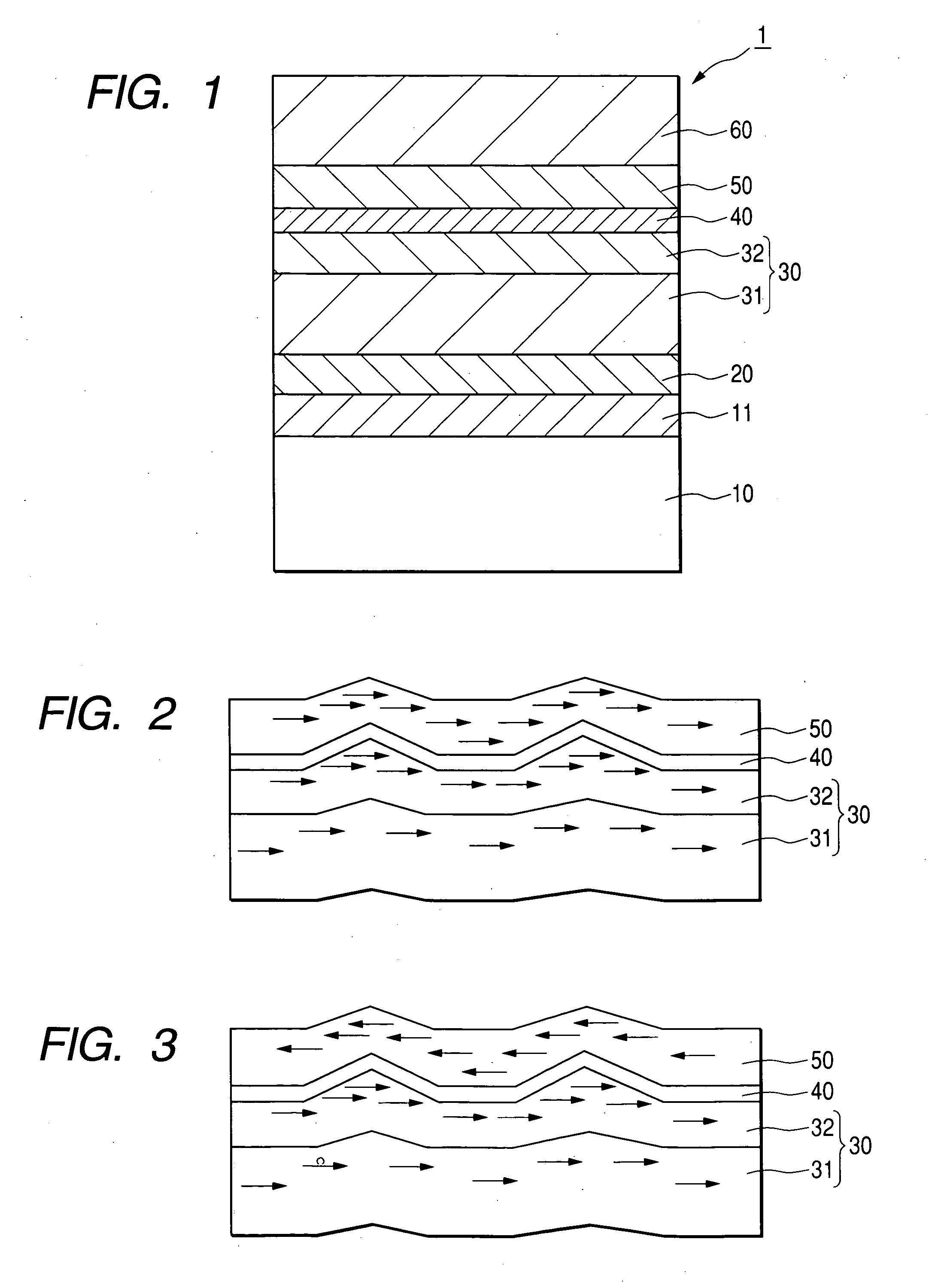
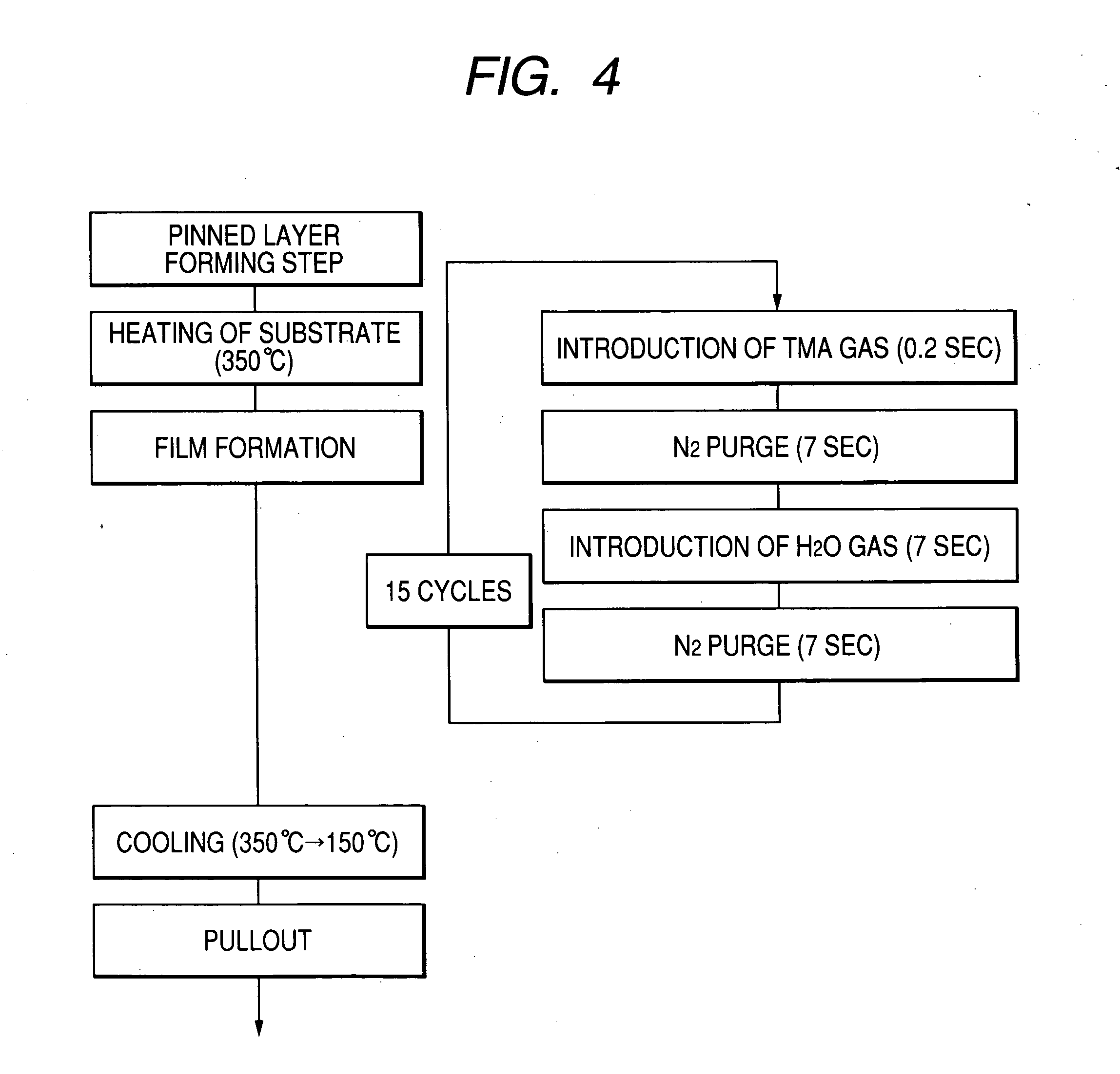
[0048]FIG. 1 is a section view of a TMR device 1 according to an embodiment of the invention. As shown in this figure, the TMR device 1 has a structure including a lower electrode layer 20, a pinned layer 30, a tunnel barrier layer 40, a free layer 50, and an upper electrode layer 60 successively formed on a substrate 10.

[0049] The substrate 10 may be a silicon substrate on which an insulating layer 11 is formed. The insulating layer 11 serves to electrically isolate the lower electrode layer 20 from the substrate 10.

[0050] The insulating layer 11 is a SiO2 thin film having a thickness of 300 nm formed on the substrate 10 by sputtering method. It is possible to form the SiO2 film by a different method, for example, by thermal oxidation of the silicon substrate 10, or by CVD (Chemical Vapor Deposition) method. The material of the insulating layer 11 is not limited to SiO2.

[0051] The lower electrode layer 20 is a Cr film formed to the thickness of 30 nm on the insulating layer 11 b...


PUM

PropertyMeasurementUnit
roughnessaaaaaaaaaa
thicknessaaaaaaaaaa
thicknessaaaaaaaaaa

Abstract

The TMR device has a structure including a lower electrode layer, a pinned layer, a tunnel barrier layer, a free layer, and an upper electrode layer which are successively formed on a substrate. The tunnel barrier layer has substantially a stoichiometric composition. The tunnel barrier layer may be a thin film of an oxide of AL formed by ALD method.

Description

CROSS-REFERENCE TO RELATED APPLICATION [0001] This application is related to Japanese Patent Application No. 2004-114243 filed on Apr. 8, 2004, the contents of which are hereby incorporated by reference. BACKGROUND OF THE INVENTION [0002] 1. Field of the Invention [0003] The present invention relates to a tunnel magnetoresistance device. [0004] 2. Description of Related Art [0005] There are a variety of electronic devices that utilize the magnetoresistance effect. MRAMs (Magnetoresistive Random Access Memories), magnetic heads, and magnetic sensors head the list of such electronic devices. [0006] Electronic devices utilizing the GMR (Giant Magnetic Resistance) effect arising from the magnetic exchange coupling between laminated magnetic thin films are also being put into commercial mass production. [0007] Meanwhile, the TMR (Tunnel MagnetoResistance) device is expected to provide highly sensitive and highly accurate electronic devices, because the MR ratio (Magnetic Resistance chang...

Claims


Application Information

Patent Timeline
Patent Type & Authority Applications(United States)
IPC IPC(8): G01R33/09G11B5/127G11B5/33G11B5/39G11C11/15H01L21/8246H01L27/105H01L43/08H01L43/10H01L43/12
CPCG11B5/39H01L43/12H01L43/08G11C11/161H10N50/10H10N50/01B82Y25/00H10B61/00
Inventor TERA, RYONOSUKETOYODA, INAOSUZUKI, YASUTOSHI
Owner DENSO CORP
Why Eureka
Try Eureka