Water-absorbing agent for organic EL device and organic EL device

a technology of organic el and water-absorbing agent, which is applied in the direction of discharge tube/lamp details, group 3/13 element organic compounds, natural mineral layered products, etc., can solve the problems of large thickness of the sealing substrate, large thickness of the sealing cap b>5/b>, and large thickness of the organic el device. achieve high reliability, stable light emission characteristics, and easy formation

Inactive Publication Date: 2005-10-13
FUTABA CORPORATION
View PDF6 Cites 40 Cited by
  • Summary
  • Abstract
  • Description
  • Claims
  • Application Information

AI Technical Summary

Benefits of technology

[0023] Since the water-absorbing agent for an organic EL device of the present invention comprises an ultraviolet curing agent and a water-absorbing substance, a water-capturing layer having desired thickness and pattern can be formed easily only by applying it to the prescribed place or part in the device and irradiating it with ultraviolet rays. According to the present invention, a large quantity of low-profile organic EL devices with a high degree of reliability, which are not affected by water or oxygen, and maintains stable light emitting characteristics for a long time can be provided.
[0024] According to the present invention, it is not necessary to form a concave portion in a sealed cap for placing a powder-like BaO or CaO or seat-like water-capturing agent using the same by molding or countersinking process, and a structure can be formed in which a light-emitting part is put between a plate-like sealed cap and a substrate on the side of an anode. Therefore, the whole thickness of the organic EL device can be made thinner, thereby making it possible to comply with a large-size with no problem. Further, according to the present invention, in the case where a concave portion in which is placed a water-capturing agent is formed in a sealed cap by molding or countersinking process, the depth of the concave portion can be made smaller. Accordingly, the whole thickness of the organic EL device can be made thinner.
[0025] According to the top-emission method of prior art, a water-capturing agent can not be placed on a cathode. According to the present invention, however, a water-absorbing agent for an organic EL device can be placed on a cathode which makes it possible to make an inorganic water-barrier layer thinner, and a manufacturing throughput can be improved and costs can be reduced.
[0026] The water-absorbing agent of the present invention can be applied to all types of organic EL devices. Accordingly, it is not necessary for EL device manufacturer to change the water-capturing agent for each different type of organic EL devices. Particularly, in the organic EL device shown in FIG. 2 having a sealed cap in which is formed a concave portion by a countersinking process, a process for packaging the water-absorbing agent for an organic EL device in the concave portion requires a coating and a UV rays-irradiation and is very easy.

Problems solved by technology

This creates such a problem that the thickness of the sealing substrate 11 or sealing cap 5 becomes large and the entire thickness of the organic EL device becomes large.
Therefore, there has been a problem that automation of assembly is hard.
Thus, the remaining water in the device or water permeating from the outside can not be captured, which makes it difficult to ensure the reliability.
However, a very high cost is required for mounting the inorganic water-barrier layer 15.
Moreover, the inorganic water-barrier layer 15 is in danger of forming a pinhole.
Therefore, depending on only the inorganic water-barrier layer 15 as water-capturing measures is not suitable for measures to ensure the reliability for mass-production.

Method used


Image

  • Water-absorbing agent for organic EL device and organic EL device
  • Water-absorbing agent for organic EL device and organic EL device
  • Water-absorbing agent for organic EL device and organic EL device

Examples


example 1

[0080] (1) Preparation of the Water-Absorbing Agent for an Organic EL Device (UV Rays-Curable Water-Capturing Agent)

[0081]“NK ester” (registered trade mark) manufactured by SHIN-NAKAMURA CHEMICAL INDUSTRIAL CO., LTD. as acrylic monomer, “Irgacure 907” (registered trade mark) manufactured by CIBA-GEIGY as an initiator and triethanolamine as an accelerator were mixed in the ratio of “Irgacure 907” to triethanolamine and to “NK ester” of 1:1:98 to form UV rays-curing agent. The same amount of the water-absorbing agent represented by the chemical structural formula (1) was added in the proportion by weight to the UV rays-curing agent, agitated and dissolved to form UV rays-curable water-capturing agent. The UV rays-curable water-capturing agent thus obtained was colorless transparent.

[0082] (2) Mounting to a Light-Emitting Part

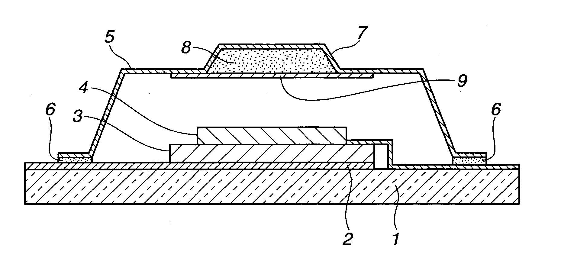
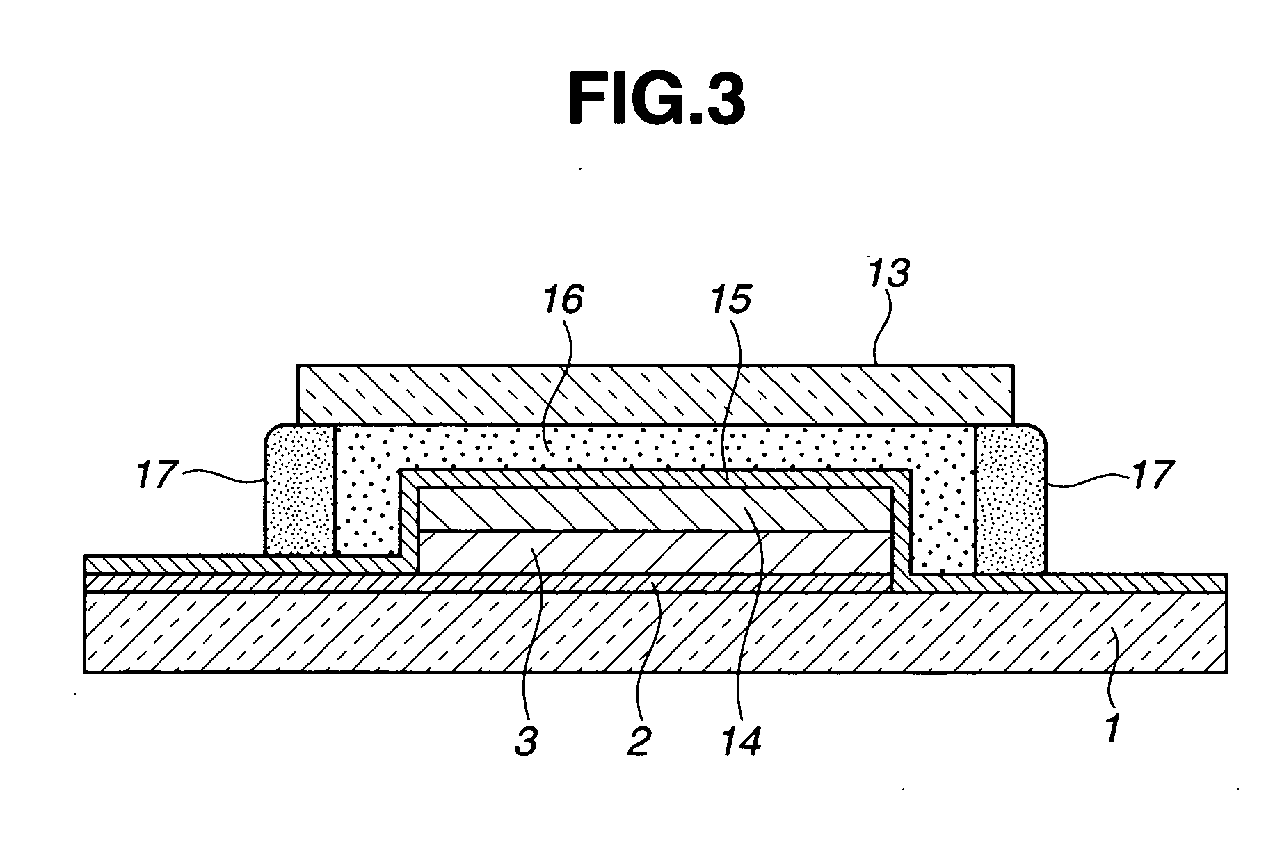
[0083] This example is relating to an organic EL device having the structure of the embodiment described with reference to FIG. 3.

[0084] ITO was formed in a d...

example 2

[0087] (1) Preparation of the Water-Absorbing Agent for an Organic EL Device (UV Rays-Curable Water-Capturing Agent)

[0088] Same as that of Example 1

[0089] (2) Mounting to a Light-Emitting Part

[0090] This example is relating to an organic EL device having the structure of the embodiment described with reference to FIG. 3.

[0091] ITO was formed in a desired pattern on a surface of the glass substrate (thickness: 0.7 mm) and placed in a vacuumed chamber. Then, a hole-injection layer, a transportation layer, an emission layer and an electron injection layer were laminated in that order on the surface of the glass substrate by a vacuum deposition method and then an Al layer (thickness: 3 nm) and an ITO layer (thickness: 30 nm) were laminated thereon to form a transparent cathode. The emission of the substrate of the organic EL device thus formed can be taken out of both the anode and cathode. The interior of a glove box was replaced by nitrogen gas to a dew point of −60° C., into whic...

example 3

[0095] (1) Preparation of the Water-Absorbing Agent for an Organic EL Device (UV Rays-Curable Water-Capturing Agent)

[0096] Same as that of Example 1

[0097] (2) Mounting to a Light-Emitting Part

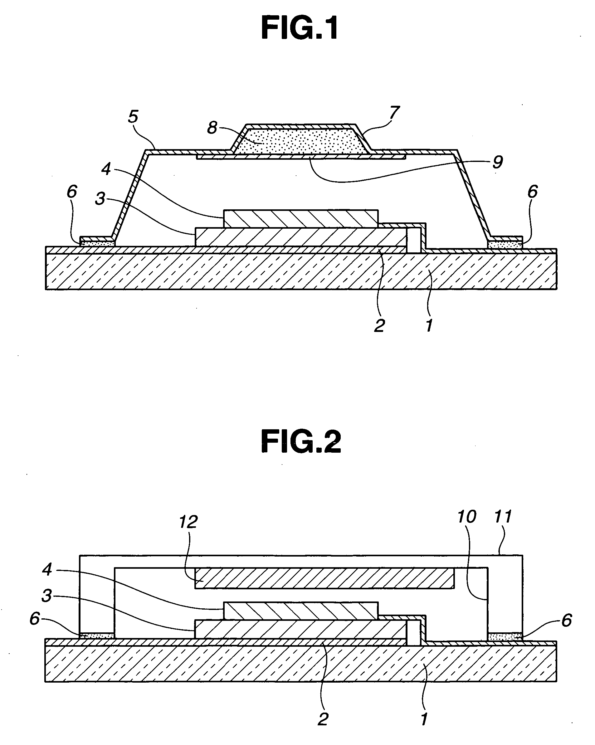
[0098] This example is relating to an organic EL device having the structure of the embodiment described with reference to FIG. 2.

[0099] ITO was formed in a desired pattern on a surface of the glass substrate (thickness: 0.7 mm) and placed in a vacuumed chamber. Then, a hole-injection layer, a transportation layer, an emission layer, an electron injection layer, and a cathode of Al, etc. were laminated in that order on the surface of the glass substrate by a vacuum deposition method to form a light-emitting part of the organic EL device. The interior of a glove box was replaced by nitrogen gas to a dew point of −60° C., into which was moved the device substrate without exposing to the air. The glass substrate (thickness: 0.7 mm) having a concave portion formed by a countersinking process (d...


PUM

PropertyMeasurementUnit
thicknessaaaaaaaaaa
thicknessaaaaaaaaaa
thicknessaaaaaaaaaa

Abstract

A thin-profile organic EL device with a high degree of reliability is provided. The anode, the organic layer and the light transmissible-type cathode are laminated on the substrate and the inorganic water-barrier layer are laminated thereon, and then a UV rays-curable type water-capturing agent comprising a UV rays-curing agent and a water-absorbing agent is cured to bond to the sealing substrate instead of an adhesive layer. The UV rays-curing agent comprises an acrylic monomer, initiator and accelerator. The UV rays-curable type sealing agent is placed to the outer peripheral portion of the UV rays-curable type water-capturing agent to be cured. The emission of the organic layer is transmitted upward via the cathode, UV rays-curable type water-capturing agent and the sealing substrate. The UV rays-curable type water-capturing agent can be formed in a desired thickness and pattern by applying it and irradiating with UV-rays, thereby making it possible to produce a low-profile organic EL device in large quantities with a high degree of reliability and without damaging the organic layer which is not resistant to water.

Description

CROSS REFERENCES TO RELATED APPLICATIONS [0001] This application claims the priority benefit of Japanese Patent Application No. 2004-114343 filed on Apr. 8, 2004. STATEMENT REGARDING FEDERALLY SPONSORED RESEARCH [0002] Not Applicable. BACKGROUND OF THE INVENTION [0003] The present invention generally relates to a water-absorbing agent and an organic EL device using the same. More particularly, the present invention relates to an improved technology making it possible to produce in large quantity a low-profile organic EL device with a high degree of reliability which is not affected by water or oxygen and maintains stable light emitting characteristics for a long time. [0004] Generally, an organic EL device is a self-light emitting device having a light-emitting part of a laminate comprising an organic EL layer formed of a thin film containing a luminescent organic compound sandwiched between an anode and a cathode. A hole and an electron are injected into the thin film containing a ...

Claims


Application Information

Patent Timeline
Patent Type & Authority Applications(United States)
IPC IPC(8): B01J20/22C07F5/06H05B33/04C08F2/44C08F20/28C09K3/00H01L23/26H01L51/50H01L51/52H05B33/14
CPCB01J20/223H01L23/26H01L51/5237H01L2924/12044Y10T428/239H01L2924/0002Y10S428/917H05B33/04H01L2924/00H10K50/846H10K50/8426
Inventor TANAKA, SATOSHIHIEDA, SHIGERUTAKAHASHI, HISAMITSUTSURUOKA, YOSHIHISA
Owner FUTABA CORPORATION
Why Eureka
Try Eureka