

Mask pattern for semiconductor device fabrication, method of forming the same, method for preparing coating composition for fine pattern formation, and method of fabricating semiconductor device
a semiconductor device and mask pattern technology, applied in the field of mask pattern formation, can solve the problems of difficult to reduce the cd of the resist pattern, material dependent and uneconomic short-wavelength exposure tool based lithography, and difficult to form contact holes less than 150 nm in size, so as to reduce the size of the opening and minimize the effect of iso-dense bias
- Summary
- Abstract
- Description
- Claims
- Application Information
AI Technical Summary
Benefits of technology
Problems solved by technology
Method used
Image

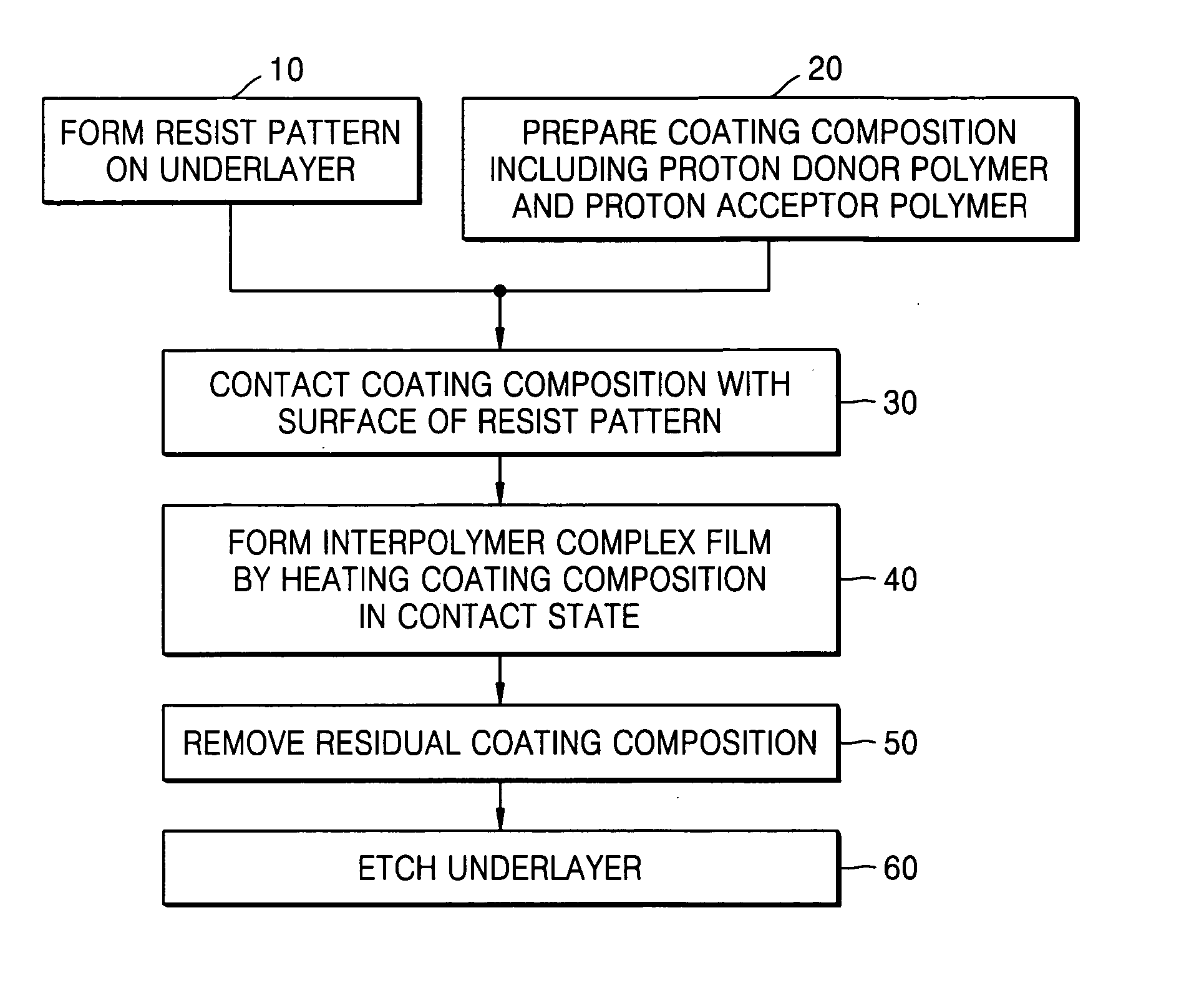
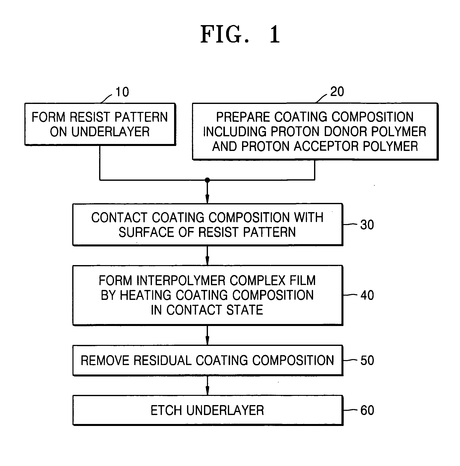
Examples
example 1
[0144] Step 1-1: Formation of Resist Pattern
[0145] An antireflective film (for example, DUV-30, Nissan Chemical Industries, Ltd.) is formed to a thickness of about 360° C. on an 8-inch bare silicon wafer. Then, a photoresist for ArF (for example, SAIL-G24c, ShinEtsu Chemical Co. Ltd) is spin-coated on the antireflective film followed by baking at about 105° C. for about 60 seconds to form a resist film with a thickness of about 3,000 Å. The resist film is exposed to light by an ArF (wavelength of 193 nm) stepper followed by post-exposure baking (PEB) at about 105° C. for about 60 seconds. Then, the wafer is developed using a 2.38 wt % tetramethylammonium hydroxide (TMAH) solution to form a resist pattern having a plurality of openings on the wafer. The resist pattern has an isolated hole pattern (hereinafter, referred to as “i-hole pattern”) with a diameter of about 129.7 nm. The resist pattern also has a dense hole pattern (hereinafter, referred to as “d-hole pattern”) with a diam...
example 2
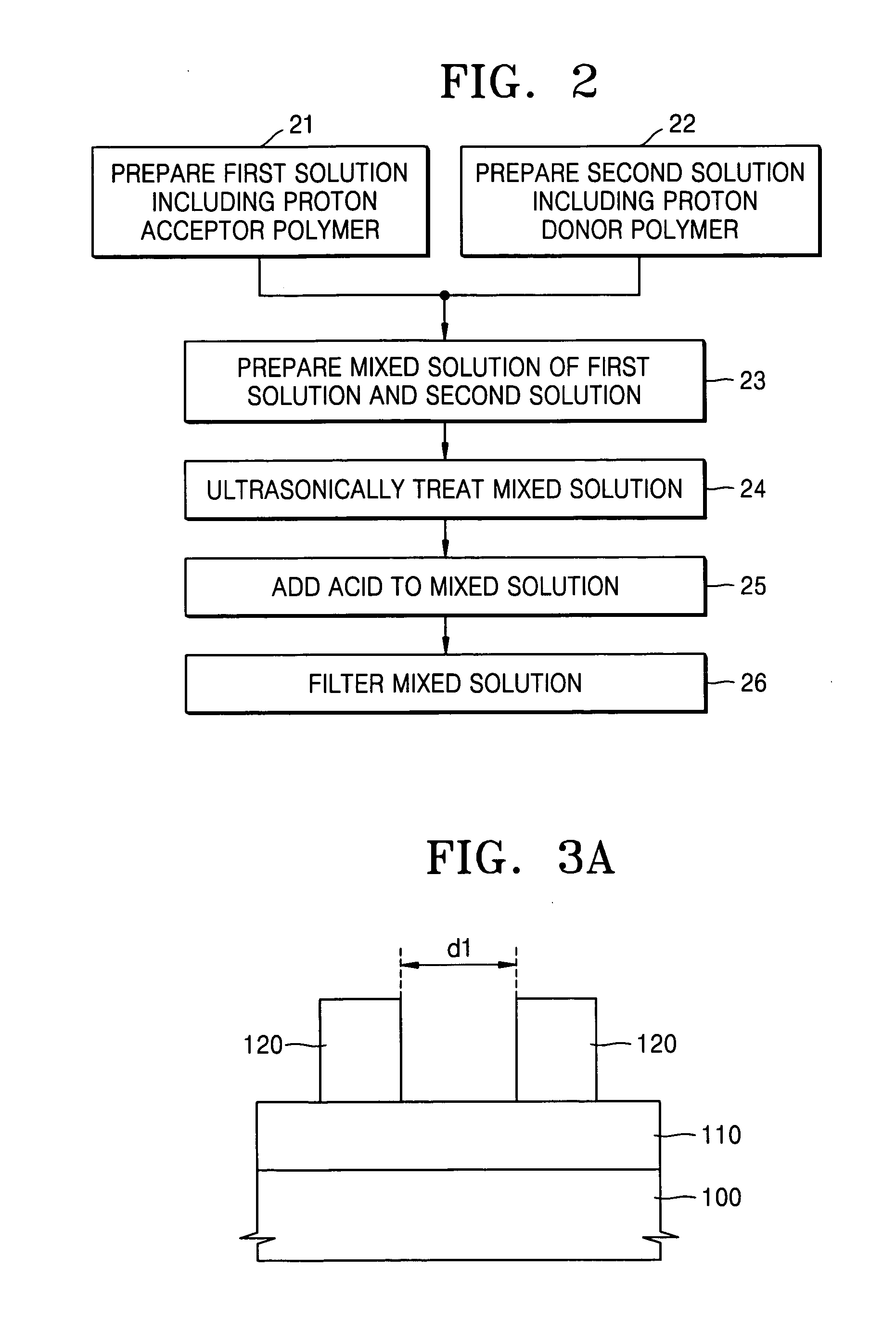
[0150] Step 2-1: Preparation of Coating Composition
[0151] A solution of about 20.0 mg of TMAH in about 2,480 mg H2O is added to a solution of about 200 mg of poly (vinylpyrrolidone) in about 1,800 mg H2O to obtain a mixed solution. About 1,500 mg H2O is further added to obtain a diluted mixed solution. A solution of about 200 mg of poly (acrylic acid) in about 1,800 mg H2O is dropwise added to the diluted mixed solution with stirring. Some precipitates and hydrogels created during the dropwise adding may be dispersed by ultrasonic treatment. About 1% aqueous solution of p-toluene sulfonic acid monohydrate is dropwise added unitil the resultant mixed solution turned cloudy. The resultant thus obtained is filtered to provide a clean coating composition.
[0152] Step 2-2: Formation of Interpolymer Complex Film
[0153] The coating composition obtained in step 2-1 is spin-coated on a resist pattern formed in substantially similar manner to step 1-1 of Example 1 to form a uniform film. The...
example 3
[0154] Step 3-1: Preparation of Coating Composition
[0155] A solution of about 32.0 mg of TMAH in about 3,968 mg H2O and a solution of about 32 mg of a thermal acid generator (for example, trade name: CYCAT4040, Cymel Co.) in about 47 mg of isopropylalcohol are added to a solution of about 200 mg of poly(vinylpyrrolidone) in about 1,800 mg H2O to obtain a mixed solution. A solution of about 200 mg of poly (acrylic acid) in about 1,800 mg H2O is dropwise added to the mixed solution with stirring. The resultant mixed solution is filtered to provide a clean coating composition.
[0156] Step 3-2: Formation of Interpolymer Complex Film
[0157] The coating composition obtained in step 3-1 is spin-coated on a resist pattern formed in substantially similar manner to step 1-1 of Example 1 to form a uniform film. The uniform film is baked at about 155° C. for about 60 seconds and rinsed with deionized water. As a result, a water-insoluble interpolymer complex film is uniformly formed on the sur...
PUM
| Property | Measurement | Unit |
|---|---|---|
| LCST | aaaaa | aaaaa |
| boiling point | aaaaa | aaaaa |
| temperature | aaaaa | aaaaa |
Abstract
Description
Claims
Application Information