

Silicon carbide semiconductor device and method for manufacturing the same
a silicon carbide semiconductor and semiconductor technology, applied in the direction of semiconductor devices, basic electric elements, electrical equipment, etc., can solve the problems of affecting the performance of the device, the eight-degree offset surface of the sic substrate is not stable, and the defect caused by polishing is easy to be generated, and achieves small on-state resistance
- Summary
- Abstract
- Description
- Claims
- Application Information
AI Technical Summary
Benefits of technology
Problems solved by technology
Method used
Image

Examples
first embodiment
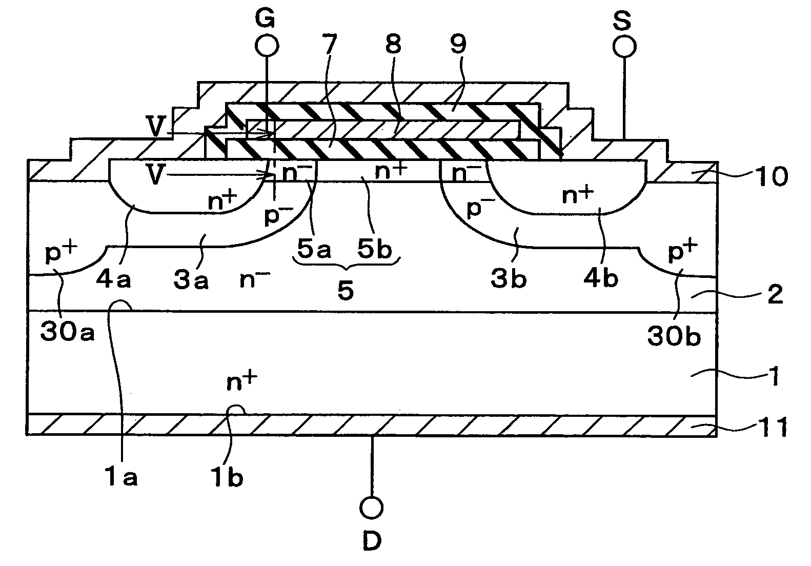
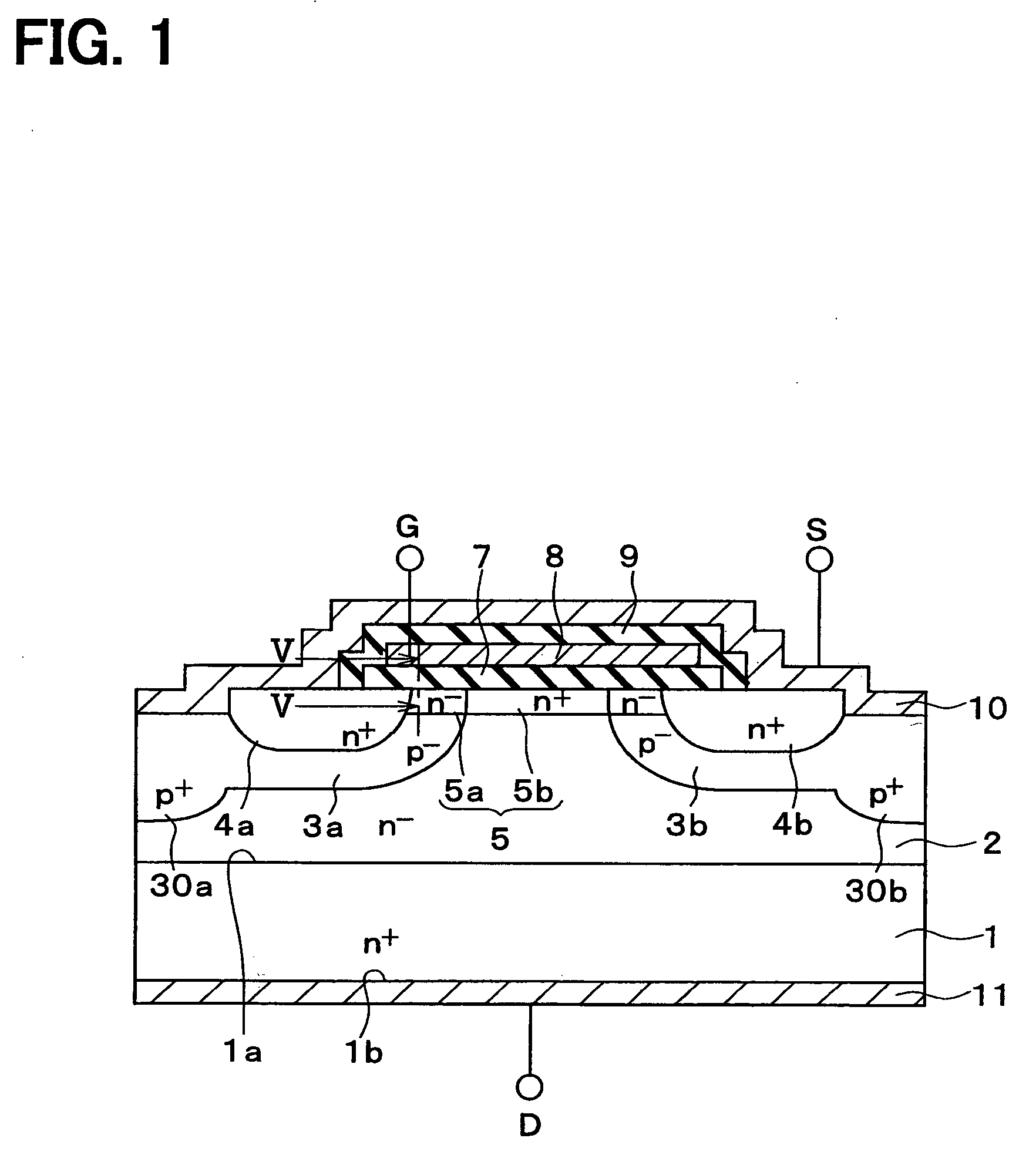
[0055]FIG. 1 is a cross sectional view showing a normally off type N channel planer type MOSFET (i.e., a vertical type power MOSFET) according to a first embodiment of the present invention. The device is suitably used for a rectifier of an alternator or an inverter of an automotive vehicle. The construction of the planer type MOSFET is described with reference to FIG. 1 as follows. Specifically, the device provides an insulation gate type field effect transistor for large amount of power.
[0056] A N+ conductive type semiconductor substrate 1 made of silicon carbide has an upper surface as a principal surface 1a, and a lower surface as a bottom surface 1b, which is opposite to the principal surface 1a. A N− conductive type epitaxial layer (i.e., a N− conductive type epitaxial layer) 2 is stacked on the principal surface 1a of the N+ conductive type semiconductor substrate 1. The N− conductive type epitaxial layer 2 is made of silicon carbide and has a dopant concentration lower than...
second embodiment
[0095] A second embodiment of the present invention is described. In this embodiment, the construction of the gate insulation film 7 is changed, compared with the first embodiment.
[0096]FIG. 6 shows a partially enlarged view showing a part of the gate insulation film 7 of the power MOSFET according to this embodiment.
[0097] As shown in this drawing, in this embodiment, the gate insulation film 7 is composed of a stacked film, which is provided by stacking the high dielectric constant film 7a and the oxide film 7b. Specifically, the gate insulation film 7 is formed in such a manner that the high dielectric constant film 7a is formed on the surface of the surface channel layer 5, and then, the oxide film 7b is formed on the surface of the high dielectric constant film 7a.
[0098]FIG. 7 shows an energy band structure in the above case. As shown in this drawing, in the high dielectric constant film 7a formed on the surface of the surface channel layer 5 made of silicon carbide, the int...
third embodiment
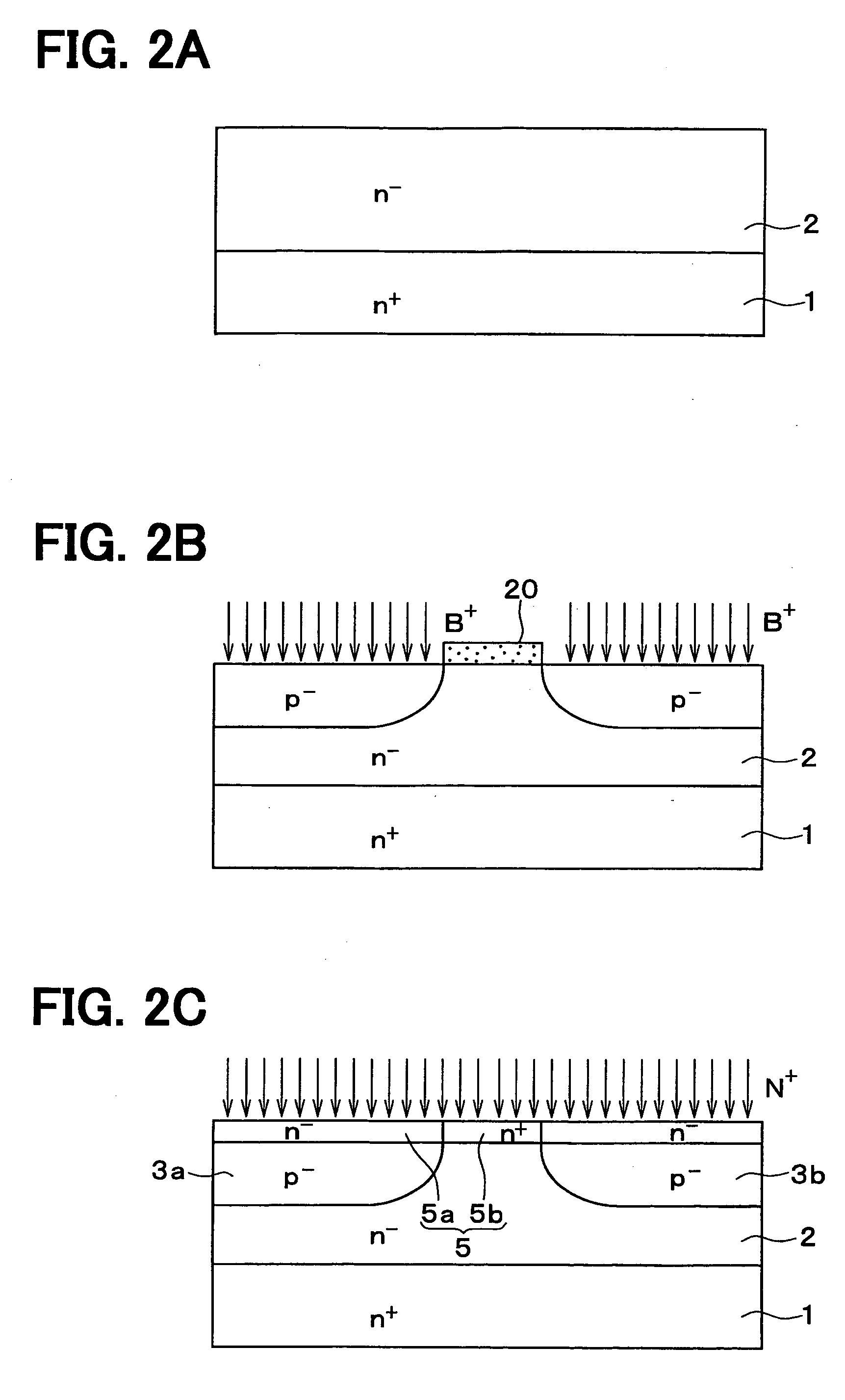
[0102] A third embodiment of the present invention is explained as follows. This embodiment is obtained by changing the surface orientation of the N− conductive type semiconductor substrate 1 in the first embodiment.
[0103] In this embodiment, the N− conductive type semiconductor substrate 1 having the principal surface tilted by 10 degrees to 20 degrees from the (0001)-Si surface is prepared. The method for manufacturing this N− conductive type semiconductor substrate 1 is explained with reference to the manufacturing process chart shown in FIGS. 8A to 8C.
[0104] Firstly, as shown in FIG. 8A, a 4H-SiC single crystal ingot having the (0001)-Si surface is prepared. Then, as shown in FIG. 8B, the ingot is cut by using a wire saw at a surface tilted by 10 degrees to 20 degrees from the (0001)-Si surface. At this time, the surface tilted by 10 degrees to 20 degrees from the (0001)-Si surface has high stability so that a mirror surface without polishing defect is obtained. Thus, the N− c...
PUM
 Abstract
Description
Claims
Application Information