CMOS image sensor

a technology of image sensor and optical field, applied in the field of optical to electronic conversion, can solve the problems of high recombination rate, short lifetime of electron-hole pair, and inability to efficiently absorb visible wavelengths

Active Publication Date: 2005-10-20
QUANTUM SEMICON
View PDF6 Cites 119 Cited by
  • Summary
  • Abstract
  • Description
  • Claims
  • Application Information

AI Technical Summary

Benefits of technology

[0022] A second object of the present invention is a process architecture to fabricate back-side illuminated color CMOS image sensors on TF-SOI or TF-GeOI substrates, in which conventional color filters are fabricated on the back-side of the buried oxide.

Problems solved by technology

Consequently, inside these semiconductor regions an electric field is very weak or completely shielded, thus leading to charge transport only through diffusion.
Since for CIS devices light is absorbed in the source / drain region of a MOSFET, the absorption of very short wavelengths (shorter than Blue) takes place very near the surface, thus the electron-hole pairs have very short lifetimes, i.e., high recombination rates.
However, conventional CCDs and CIS devices utilize the bulk of the silicon wafer for photo-absorption, while with Thin-Film SOI the top silicon film, which is used to make CMOS devices, cannot efficiently absorb wavelengths in the visible, because it is too thin, i.e., the optical path inside the absorption film is too short.
Therefore, it can be said that conventional CIS technology is fundamentally incompatible with Thin-Film SOI substrates, and consequently incompatible with the requirements for high performance sub-90 nm CMOS technologies.
It can then be concluded that conventional CMOS image sensors will not be able to take advantage of the well known benefits of CMOS scaling, also known as “Moore's Law”, in terms of speed, density, power dissipation and cost.
The inability to scale the size of CMOS devices will ultimately result in the impossibility to scale the size of pixels of CIS.
Consequently this will also put a limitation on how small the entire image sensor can be for a given resolution, which in turn places constraints on the design of the optical system (lenses), thereby impacting the overall system size, weight, cost, etc.
The scaling of the pixel size of CMOS image sensors is also limited by the resolution of the lens system.
It is therefore pointless to scale the pixel size below what the lens system can resolve.
On the other hand the cost of a lens system increases for higher resolution lenses.
This means that it is not possible to design a lens system having a resolution approaching the wavelength of the light that it is meant to focus, even with the non-realistic assumption that the lenses could be manufactured with infinite precision.
However, even if such junctions did exist on Thin-Film SOI CMOS devices, since the crystalline silicon film is so thin, typically less than 30 nm, the absorption of light in the visible range would be very inefficient, and insufficient to be of practical use for image sensors.
The limitation on the number of metal levels places severe consequences on the “system architecture” that can be fabricated on the same die, thus monolithically integrated, with the image sensors.
“Front-side” illumination also requires the light sensing regions not to be blocked by metal lines, thereby placing severe restrictions on the metal lines connecting the in-pixel circuitry to the peripheral circuitry.
This limitation to the metal interconnects between the pixels and the periphery limits the maximum bandwidth available for the pixel-to-periphery communications, which in turn has detrimental consequences for parameters such as maximum frame rate, dynamic range, etc.
It must be emphasized that any of these structures per se, or combined in some fashion, are impossible to implement with bulk substrates.

Method used


Image

  • CMOS image sensor
  • CMOS image sensor
  • CMOS image sensor

Examples


Embodiment Construction

[0038] Back-Side Illuminated TF-SOI CMOS Image Sensors

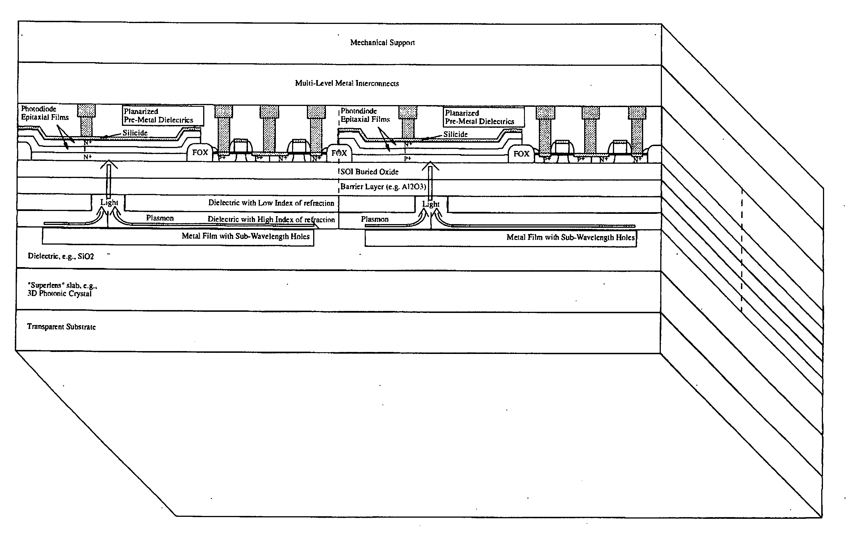
[0039] The innovations disclosed in WO 02 / 033755 and co-pending application PCT / EP / 03 / 10346, which are incorporated herein by way of reference, can be combined to generate a completely new kind of CMOS Imager Sensor (CIS) in which SAM-APDs are made on TF-SOI or TF-GeOI. FIG. 1 shows a schematic representation of a fully processed TF-SOI wafer, in which the CMOS devices, the photo-diode layer, and the complete metallization stack have been made.

[0040] In SOI and GeOI substrates, the wafer under the buried oxide is used only as a mechanical support for the buried oxide and top crystalline semiconductor (Si or Ge) films, and it has very little impact on the properties of the CMOS devices to be fabricated on the top crystalline semiconductor film. For this reason the wafer bulk under the buried oxide can easily be replaced by a different mechanical substrate that is transparent to light in wavelengths of interest, such as the UV, V...


PUM


Abstract

Light sensing devices are monolithically integrates with CMOS devices on Thin-Film Silicon-On-insulator (TF-SOI) or Thin-Film Germanium-On-Insulator (TF-GeOI) substrates. Photodiode active layers are epitaxially grown on the front-side of the substrate and after full processing of the front-side of the substrate, the substrate material is removed under the buried insulator (buried oxide). Monolithically integrated structures are then fabricated on the back of the buried oxide. The back-side is then bonded to a new substrate that is transparent to the wavelengths of interest. For example, quartz, sapphire, glass, or plastic, are suitable for the visible range. Back-side illumination of the sensor matrix is thereby allowed, with light traveling through the structures fabricated on the back of the substrate, opposite to the side on which CMOS is made.

Description

BACKGROUND OF THE INVENTION [0001] The present invention relates to methods of optical to electronic conversion, in particular to photo-detection with silicon-based devices suitable for integration with Complementary Metal Oxide Semiconductor (CMOS) technology. [0002] Conventional Charge Coupled Devices (CCDs) and CMOS image sensors (CIS) comprise several elements that are key to high performance image sensing. The photo-diode, which converts light into electrical signals, the CMOS devices and circuits that handle the analog signal, convert it to a digital signal, and that perform digital signal processing, the color filters, etc. CIS technology has the advantage that all these elements can be monolithically integrated on the same “die” or “chip”, while CCDs can only monolithically integrate color filtering and photo-absorption. [0003] In conventional CIS technology the built-in vertical pn-junctions, source-to-well and drain-to-well junctions, formed during the fabrication of the C...

Claims


Application Information

Patent Timeline
Patent Type & Authority Applications(United States)
IPC IPC(8): G02B5/18G02B5/20H01L27/12H01L27/14H01L27/146H01L31/105
CPCG02B1/005H01L27/1464G02B5/201G02B5/208H01L27/12H01L27/14609H01L27/14618H01L27/14621H01L27/14625H01L27/1463H01L27/14636H01L27/14643H01L31/02165H01L31/105G02B5/008H01L2924/0002H01L2924/00
Inventor AUGUSTO, CARLOS J.R.P.
Owner QUANTUM SEMICON
Why Eureka
Try Eureka