Laser irradiation apparatus and method for manufacturing semiconductor device

a laser irradiation and semiconductor technology, applied in the direction of instruments, recording signal processing, disposition/mounting of heads, etc., can solve the problems of low density of photon to time, low output power per unit time of continuous wave laser, and low density of pulsed laser. achieve the effect of increasing the throughput of laser irradiation

Inactive Publication Date: 2005-10-27
SEMICON ENERGY LAB CO LTD
View PDF18 Cites 58 Cited by
  • Summary
  • Abstract
  • Description
  • Claims
  • Application Information

AI Technical Summary

Benefits of technology

[0014] In view of the above problems, it is an object of the present invention to provide a laser irradiation apparatus which can irradiate an irradiation object with a linear beam spot having homogeneous energy density in the major-axis direction without complicating the optical system. It is another object of the present invention

Problems solved by technology

However, these optical elements for homogenizing the energy density have a problem in that the adjustment is complicate because they require advanced optical design in consideration of a wavefront and a shape of the beam spot.
However, the continuous wave laser has lower output power per unit time than the pulsed laser.
Therefore, the density of photon to time is also low, and the conversion efficiency into the harmonic by the non-linear optical element is also low.
The continuous wave laser has another problem in that the resistance of the non-linear optical

Method used


Image

  • Laser irradiation apparatus and method for manufacturing semiconductor device
  • Laser irradiation apparatus and method for manufacturing semiconductor device
  • Laser irradiation apparatus and method for manufacturing semiconductor device

Examples


embodiment mode 1

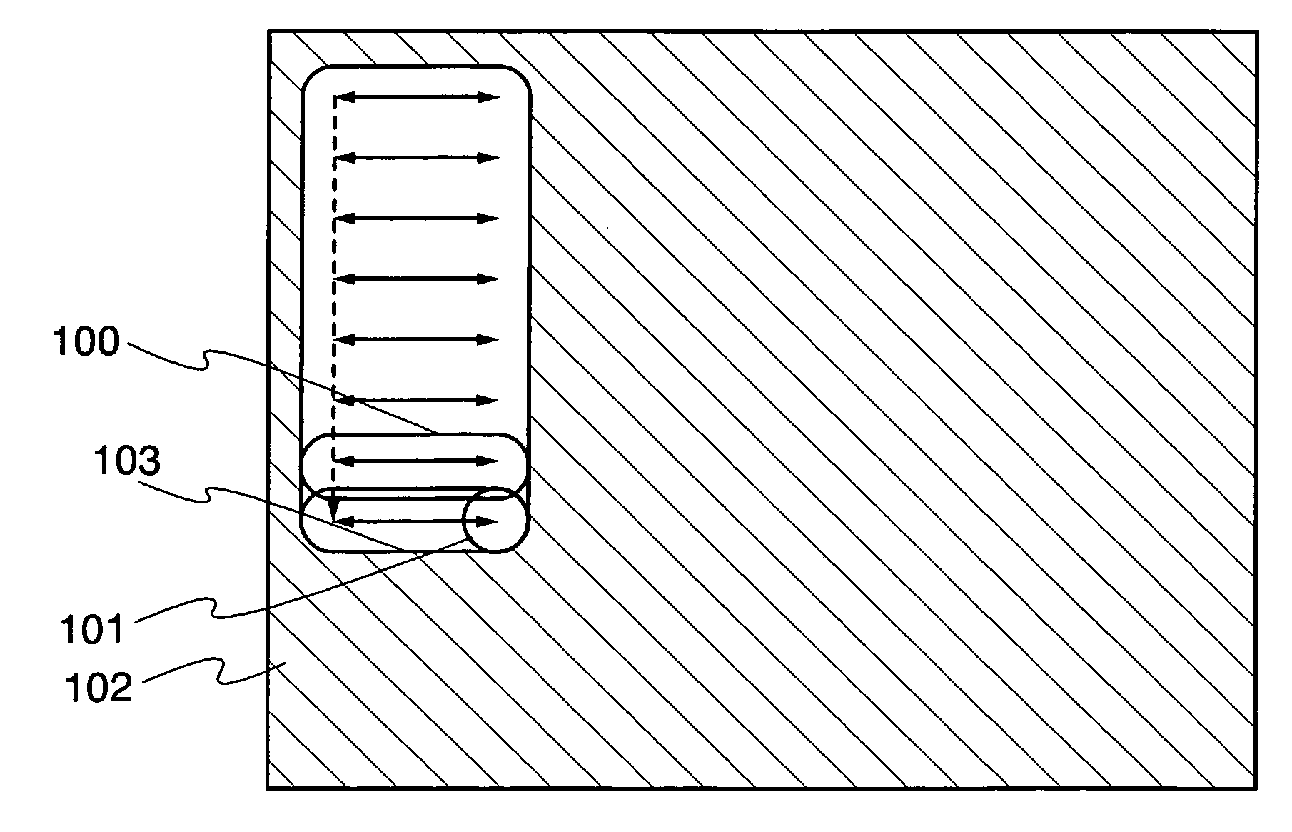
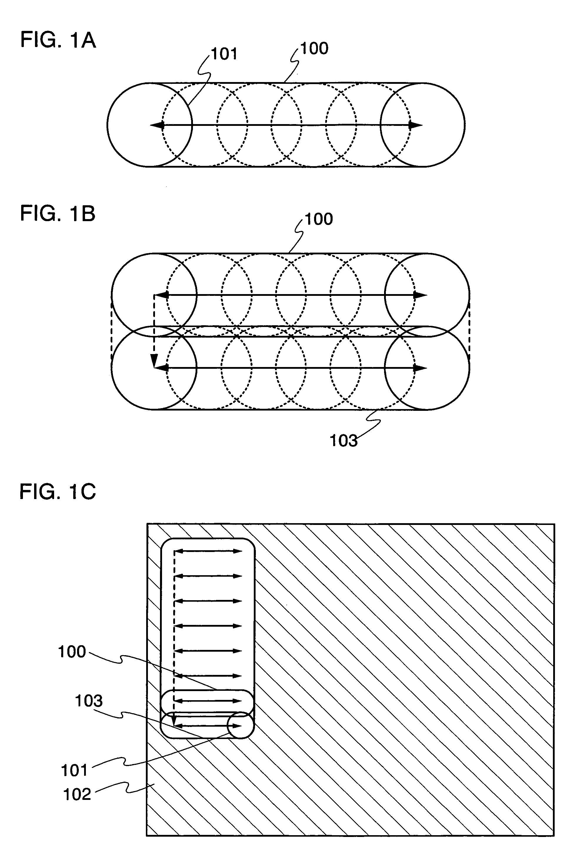
[0055] A step of forming a quasi-linear beam spot used in the present invention is described with reference to FIGS. 1A to 1C. As shown in FIG. 1A, a quasi-linear beam spot 100 is formed by scanning a beam spot 101 of the laser beam in a uniaxial direction or along a straight line as indicated by a solid-line arrow.

[0056] In FIG. 1A, the quasi-linear beam spot 100 is formed by scanning the beam spot 101 so as to move it back and forth. However, the present invention is not limited to this configuration, and the quasi-linear beam spot 100 may be formed by scanning the beam spot 101 in only one direction. Moreover, FIG. 1A illustrates the quasi-linear beam spot 100 formed in such a way that after the beam spot 101 is scanned from left to right, it is scanned from right to left again. However, the present invention is not limited to this configuration. In the present invention, the beam spot 101 may be scanned at least once in any one point in the quasi-linear beam spot 100.

[0057] In...

embodiment mode 2

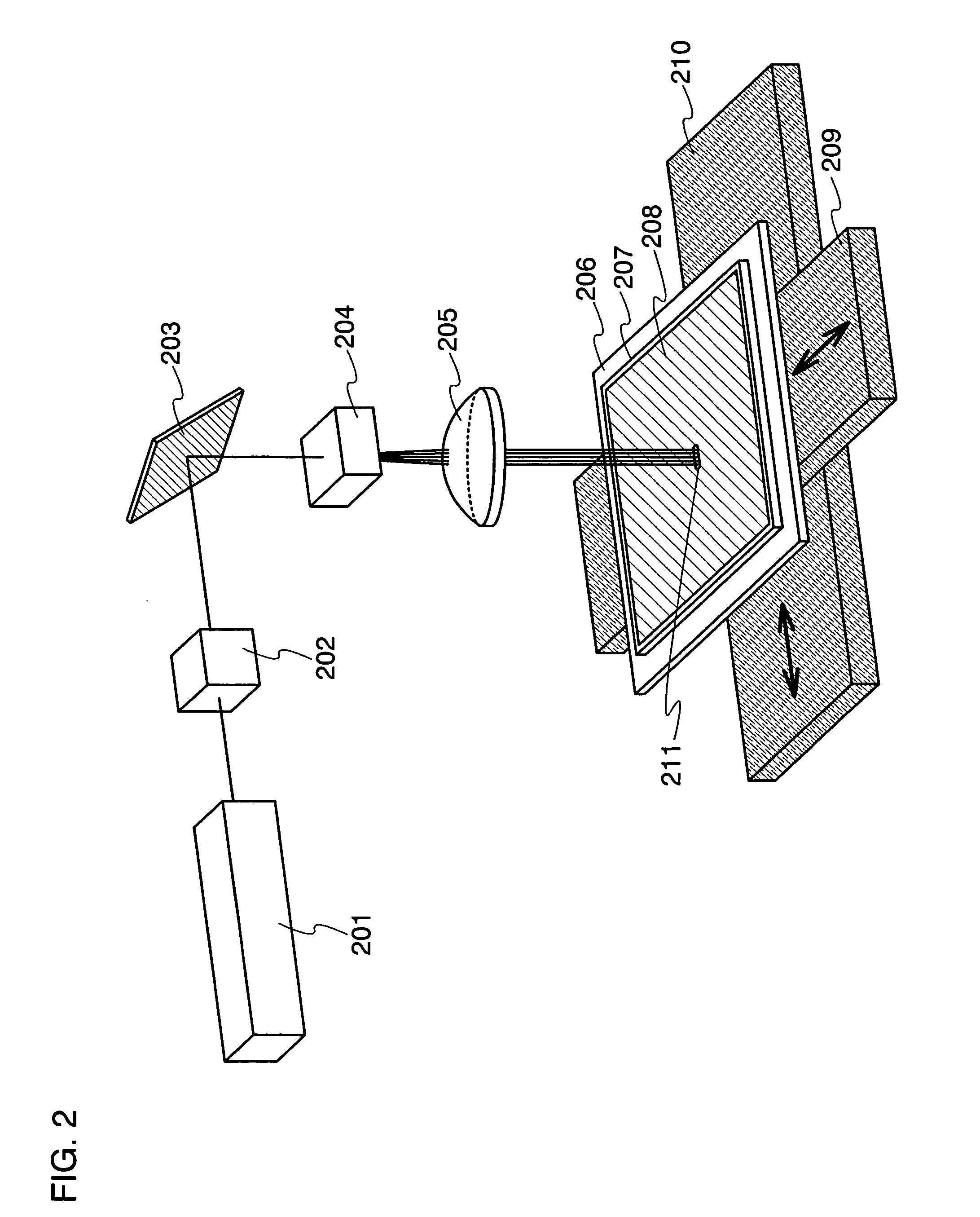
[0083] With reference to FIGS. 11A to 11C, this embodiment mode describes a scanning method of the laser beam which is different from the scanning method shown in the embodiment mode 1. Other parts of this embodiment mode except the scanning method of the laser beam are the same as those in the embodiment mode 1. The laser irradiation apparatus shown in FIG. 2 is used in this embodiment mode.

[0084] In FIGS. 11A to 11C, reference numerals 1101 and 1102 denote quasi-linear beam spots, reference numerals 1103 and 1104 denote beam spots, and a reference numeral 1105 denotes a semiconductor film, which is the irradiation object. By scanning the beam spot shown in FIGS. 11A to 11C, the quasi-linear beam spot is formed in the same way as the embodiment mode 1. The quasi-linear beam spot 1101 and the quasi-linear beam spot 1102, which is formed sequentially after the quasi-linear beam spot 1101, are scanned so that regions in these beam spots parallel to their major axes overlap each other...

embodiment mode 3

[0091] Another embodiment mode of the present invention is described.

[0092] First, the step of forming a quasi-linear beam spot used in the present invention is described with reference to FIGS. 4A to 4C. FIG. 4A shows a quasi-linear beam spot 300 formed by scanning a beam spot 301 of a laser beam in one direction or along a straight line as indicated by a solid-line arrow.

[0093] In FIG. 4A, unlike the embodiment mode 1, the beam spot 301 is scanned only in one direction to form the quasi-linear beam spot 300. The total time of laser irradiation can be homogenized in any one point within the quasi-linear beam spot 300 by scanning the beam spot 301 only in one direction as shown in FIG. 4A. Although FIG. 4A illustrates the beam spot 301 scanned from left to right, the present invention is not limited to this configuration. In the present invention, the beam spot 301 may be scanned at least once in any one point within the quasi-linear beam spot 300.

[0094] In the case of FIG. 4A, t...


PUM

PropertyMeasurementUnit
Timeaaaaaaaaaa
Frequencyaaaaaaaaaa

Abstract

It is an object of the present invention to provide a laser irradiation apparatus being able to irradiate the irradiation object with the laser beam having homogeneous energy density without complicating the optical system. The laser irradiation apparatus of the present invention comprises a laser oscillator, an optical system for scanning repeatedly a beam spot of the laser beam emitted from the laser oscillator in a uniaxial direction over the surface of the irradiation object, and a position controlling means for moving the position of the irradiation object relative to the laser beam in a direction perpendicular to the uniaxial direction.

Description

BACKGROUND OF THE INVENTION [0001] 1. Field of the Invention [0002] The present invention relates to a laser irradiation apparatus used for crystallizing a semiconductor film. Moreover, the present invention relates to a method for manufacturing a semiconductor device. [0003] 2. Related Art [0004] A thin film transistor (TFT) formed using a poly-crystalline semiconductor film is higher in mobility by double digits or more than a TFT formed using an amorphous semiconductor film, and has an advantage that a pixel portion and a peripheral driver circuit in a semiconductor display device can be integrally formed over the same substrate. The poly-crystalline semiconductor film can be formed over an inexpensive glass substrate by employing a laser annealing method. [0005] As laser oscillators used in the laser annealing method, there are a pulsed laser oscillator and a continuous wave laser oscillator according to the oscillation method. The pulsed laser oscillator typified by an excimer ...

Claims


Application Information

Patent Timeline
IPC IPC(8): B23K26/073G11B7/08H01L21/20H01L21/268H01L21/324H01L21/336H01L21/77H01L27/32H01L29/786H01L51/52
CPCB23K26/0738B23K26/0807B23K26/0815B23K26/0853H01L27/1285H01L21/268H01L27/3244H01L27/3295H01L51/5237H01L21/2026B23K26/0821B23K26/082H01L21/02672H01L21/02691H01L21/02683H01L21/02686H01L21/02532H10K59/122H10K59/12H10K50/844H01L21/26H01S3/10
Inventor TANAKA, KOICHIROYAMAMOTO, YOSHIAKI
Owner SEMICON ENERGY LAB CO LTD
Why Eureka
Try Eureka