Pulsed magnetron for sputter deposition

a sputter and magnetron technology, applied in the field of sputtering, can solve the problems of adversely affecting the formation of the underlying silicide, difficult to achieve thin films with a desired degree of uniformity, and the relative height of the vertical structure is growing increasingly tall

Inactive Publication Date: 2005-11-10
APPLIED MATERIALS INC
View PDF3 Cites 23 Cited by
  • Summary
  • Abstract
  • Description
  • Claims
  • Application Information

AI Technical Summary

Problems solved by technology

However, such thin films are often difficult to achieve with a desired degree of uniformity over nonplanar structures such as those shown in FIG. 1.
These thinner areas may adversely affect the formation of the underlying silicide.
In addition, the relative height of the vertical structures is growing increasingly tall.
As the vertical to horizontal aspect ratio of these gate spacing holes between adjacent gates becomes increasingly large, achieving satisfactory coverage of the source and drain regions at the bottoms of such deep holes is made more difficult...

Method used


Image

  • Pulsed magnetron for sputter deposition
  • Pulsed magnetron for sputter deposition
  • Pulsed magnetron for sputter deposition

Examples


Embodiment Construction

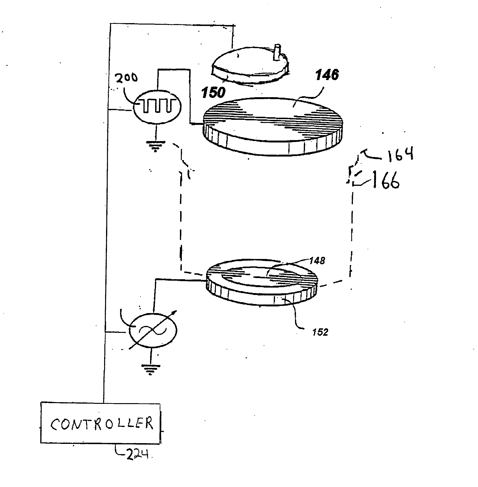
[0019] One embodiment of the present inventions is directed to sputter depositing a metal layer by biasing a sputter target with pulsed power in which the power applied to the target alternates between low and high levels. The high levels are, in one embodiment, sufficiently high to maintain a plasma for ionizing deposition material. The low levels are, in one embodiment, sufficiently low such that the power applied to the target during the high and low levels is, on average, low enough to facilitate deposition of thin layers if desired.

[0020] In the illustrated embodiment, the power applied to bias the target is modulated in a plurality of alternating first and second intervals wherein in each of the first intervals, the power level is at a first level sufficiently high to attract ions to sputter the target. In each of the second intervals, the power is applied at a second level higher than the first level and sufficiently high not only to sputter the target but also to maintain a...


PUM

PropertyMeasurementUnit
Fractionaaaaaaaaaa
Frequencyaaaaaaaaaa
Frequencyaaaaaaaaaa

Abstract

A magnetron sputter reactor for sputtering deposition materials such as nickel and cobalt, for example, and its method of use, in which self-ionized plasma (SIP) sputtering is promoted. SIP is promoted by a small magnetron having poles of unequal magnetic strength and a high power applied to the target during sputtering. One embodiment of the present inventions is directed to sputter depositing a metal layer by biasing a sputter target with pulsed power in which the power applied to the target alternates between low and high levels. The high levels are, in one embodiment, sufficiently high to maintain a plasma for ionizing deposition material. The low levels are, in one embodiment, sufficiently low such that the power applied to the target during the high and low levels is, on average, low enough to facilitate deposition of thin layers if desired.

Description

FIELD OF THE INVENTION [0001] The inventions relate generally to sputtering. In particular, the invention relates to the sputter deposition of material in the formation of semiconductor integrated circuits. BACKGROUND ART [0002] Semiconductor integrated circuits such as complementary metal oxide silicon (CMOS) devices may include a silicide layer to provide low sheet resistance on gate, source or drain regions. A silicide is a compound formed in a reaction between a metal and silicon or polysilicon. In addition to CMOS, silicide can be a useful component of a variety of other semiconductor devices, particularly where a low sheet resistance or low contact resistance is desired. [0003] Various metals may be deposited on silicon or polysilicon to react with the underlying silicon to form the silicide. Titanium is commonly reacted with silicon to form titanium silicide, TiSi2. It has also been proposed to use cobalt and nickel to form silicides. [0004]FIG. 1 shows a metal layer 10 which...

Claims


Application Information

Patent Timeline
IPC IPC(8): C23C14/34H01J37/34H01L21/285
CPCC23C14/34H01J37/32706H01L21/2855H01J2237/3327H01J37/3408
Inventor SAIGAL, DINESHFORSTER, JOHN C.LAI, SHUK YING
Owner APPLIED MATERIALS INC
Why Eureka
Try Eureka