Semiconductor device
a technology of semiconductor devices and semiconductors, applied in semiconductor devices, semiconductor/solid-state device details, electrical apparatus, etc., can solve the problems of difficult to induce enough carrier in the channel region, the threshold voltage is increased, and the electric field cannot be applied to the gate, etc., to achieve the control of the threshold voltage of the p-type mosfet
- Summary
- Abstract
- Description
- Claims
- Application Information
AI Technical Summary
Benefits of technology
Problems solved by technology
Method used
Image

Examples
first embodiment
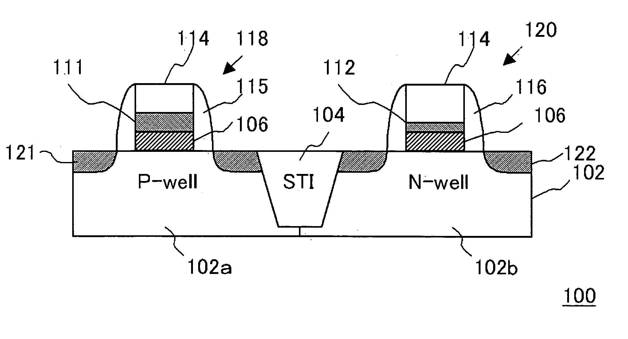
[0043]FIG. 1 is a cross-sectional view, illustrating a configuration of a semiconductor device in this embodiment.
[0044] In this embodiment, the semiconductor device 100 is a complementary metal oxide semiconductor (CMOS) device including an N-type MOSFET 118 and a P-type MOSFET 120. In addition, this CMOS device composes an internal circuit of a LSI.
[0045] The semiconductor device 100 comprises a silicon substrate 102, which has a P-well 102a of P-type conductivity and an N-well 102b of N-type conductivity provided thereon and a device separating-region 104 for separating the P-well 102a from the N-well 102b. An N-type MOSFET 118 and a P-type MOSFET 120 are formed in the P-well 102a and the N-well 102b, respectively.
[0046] A pair of impurity diffusion regions 121 is provided in the P-well 102a, and a channel region is formed therebetween. On the channel region is provided with a gate, which comprises a gate insulating film having a silicon oxide film 106 and a first high dielect...
second embodiment
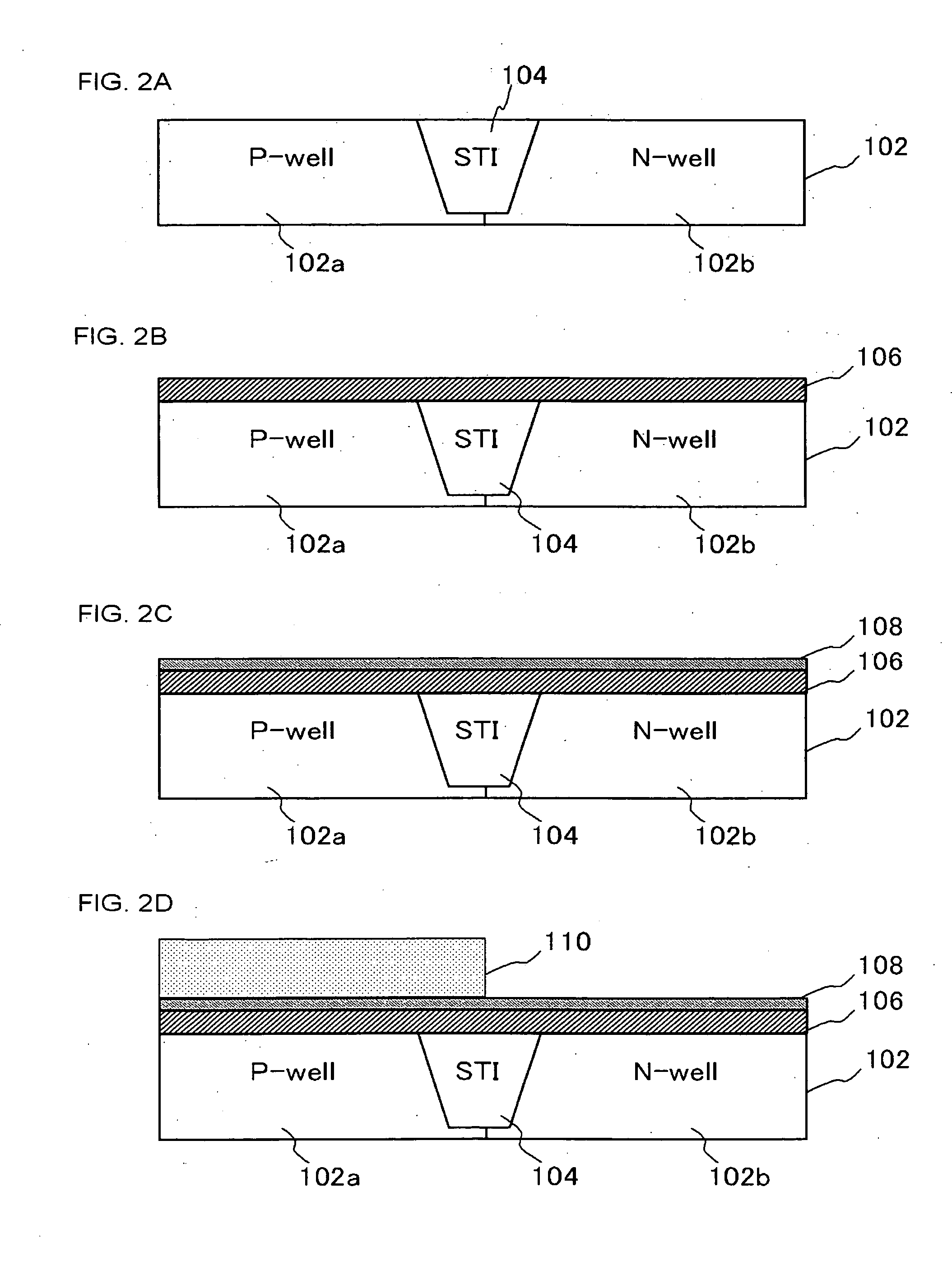
[0067] In this embodiment, similar process as described in the first embodiment in reference to FIG. 2A to FIG. 2D is conducted, and more specifically the silicon oxide film 106 and the high dielectric constant film 108 are formed on the silicon substrate 102 and the photo resist 110 is formed over the P-well 102a. A wet etching process is conducted by using, for example, diluted fluorinated acid (DHF) to selectively remove the high dielectric constant film 108 and the silicon oxide film 106 on the N-well 102b (FIG. 4). The present embodiment is different from the first embodiment in the point that the silicon oxide film 106 is also removed with the high dielectric constant film 108.
[0068] Subsequently, the photo resist 110 is removed and thereafter, a thermal oxidation is conducted on the surface of the N-well 102b of the silicon substrate 102 to form a silicon oxide film (not shown) on the N-well 102b. Subsequently, the high dielectric constant film is formed on the silicon oxide...
example
[0072] The P-type MOSFET 120 described in the first embodiment and having the configuration shown in FIG. 1 was employed to investigate a relationship of the film thickness of the second high dielectric constant film 112 with the threshold voltage in the P-type MOSFET 120. The results thereof are shown in FIG. 6.
[0073] As can be seen in the graph, thicker film thickness of the second high dielectric constant film 112 provides an increase of the threshold voltage in the P-type MOSFET 120. It was exhibited that the threshold voltage was in a level that is applicable to the manufacturing application (not higher than about 0.5 V) when the film thickness of the second high dielectric constant film 112 was equal to or less than 1 nm. In addition, it was found that the increase of the threshold voltage could be more effectively controlled by providing the film thickness of the second high dielectric constant film 112 as not greater than 0.5 nm. The P-type MOSFETs 120 having different film...
PUM
 Abstract
Description
Claims
Application Information
 - R&D
- Intellectual Property
- Life Sciences
- Materials
- Tech Scout
- Unparalleled Data Quality
- Higher Quality Content
- 60% Fewer Hallucinations
Browse by: Latest US Patents, China's latest patents, Technical Efficacy Thesaurus, Application Domain, Technology Topic, Popular Technical Reports.
© 2025 PatSnap. All rights reserved.Legal|Privacy policy|Modern Slavery Act Transparency Statement|Sitemap|About US| Contact US: help@patsnap.com