Nitride semiconductor device

a technology of nitride and semiconductors, applied in the direction of semiconductor devices, basic electric elements, electrical apparatus, etc., can solve the problems of large diameter substrates, large diameter substrates, and expensive substrates

Inactive Publication Date: 2005-12-15
KK TOSHIBA
View PDF3 Cites 160 Cited by
  • Summary
  • Abstract
  • Description
  • Claims
  • Application Information

AI Technical Summary

Problems solved by technology

Since it is difficult to manufacture a substrate made of single gallium nitride in the aluminum gallium nitride / gallium nitride heterostructure, the substrate is generally formed by crystal growth on a substrate such as a sapphire substrate or a silicon carbide (SiC) substrate.
However, there is a problem that, since the sapphire substrate has large thermal resistance, radiation from a device formed on the substrate is difficult, and further there is a problem that the substrate having a large diameter is difficult to manufacture so that even the substrate having a small diameter on the order of 2 to 3 inches is expensive.
On the other hand, no problem occurs on the radiation from a device formed on the substrate because the silicon carbide substrate has small thermal resistance, but there is a problem that the substrate having a large diameter is difficult to manufacture like the sapphire substrate and even the substrate having a small diameter is expensive.
Since the upper limit of the breakdown voltage of the gallium nitride layer contained device on the silicon substrate is determined depending on the thickness of the gallium nitride layer, the breakdown voltage of at most about 200 V can be secured at present, and a nitride semiconductor device having a high breakdown voltage of 600V, 1200 V, or more is difficult to achieve.
However, in the method disclosed in Japanese Patent Application Laid-Open No. 2003-17409 Publication, a warpage prevention layer is formed on the semiconductor layer so that a structural limitation is imposed on the semiconductor device.
Therefore, when a semiconductor layer having greatly different lattic constant or thermal expansion coefficient is formed on the semiconductor substrate having a large diameter, a problem that crack or warpage easily occurs on the substrate cannot still solved basically.

Method used


Image

  • Nitride semiconductor device
  • Nitride semiconductor device
  • Nitride semiconductor device

Examples


first embodiment

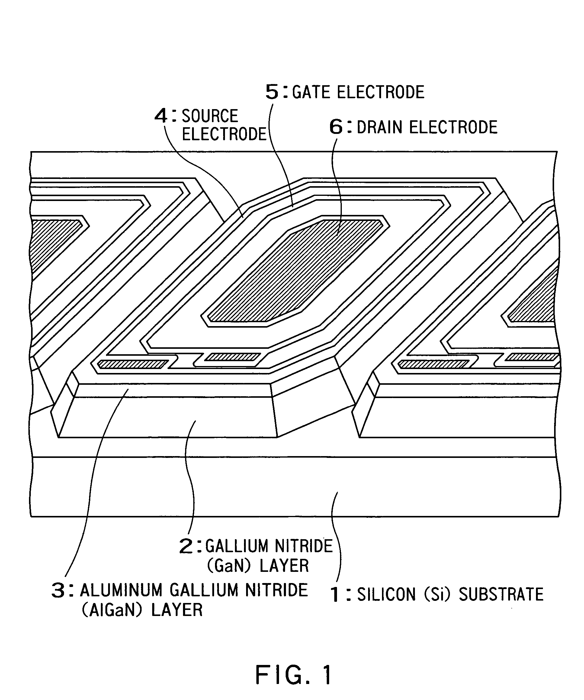
[0028]FIG. 1 is a perspective view schematically showing a structure of a nitride semiconductor device according to the present invention.

[0029] The nitride semiconductor device according to the first embodiment of the present invention comprises a silicon (Si) substrate 1, a gallium nitride (GaN) layer 2 as a first aluminum gallium nitride (AlxGa1-xN (0≦x≦1)) layer formed on the silicon substrate 1 in an island shape, and an aluminum gallium nitride (AlGaN) layer 3 as a second aluminum gallium nitride (AlyGa1-yN (0≦y≦1, x2.

[0030] The gallium nitride layer 2 is a semiconductor layer functioning as a channel layer, and may be formed as an i (intrinsic)-type gallium nitride layer.

[0031] The aluminum gallium nitride layer 3 is a semiconductor layer functioning as a barrier layer which supplies electrons to the channel layer, and may be formed as an n-type or i-type aluminum gallium nitride layer.

[0032] The nitride semiconductor device according to the first embodiment of the present...

second embodiment

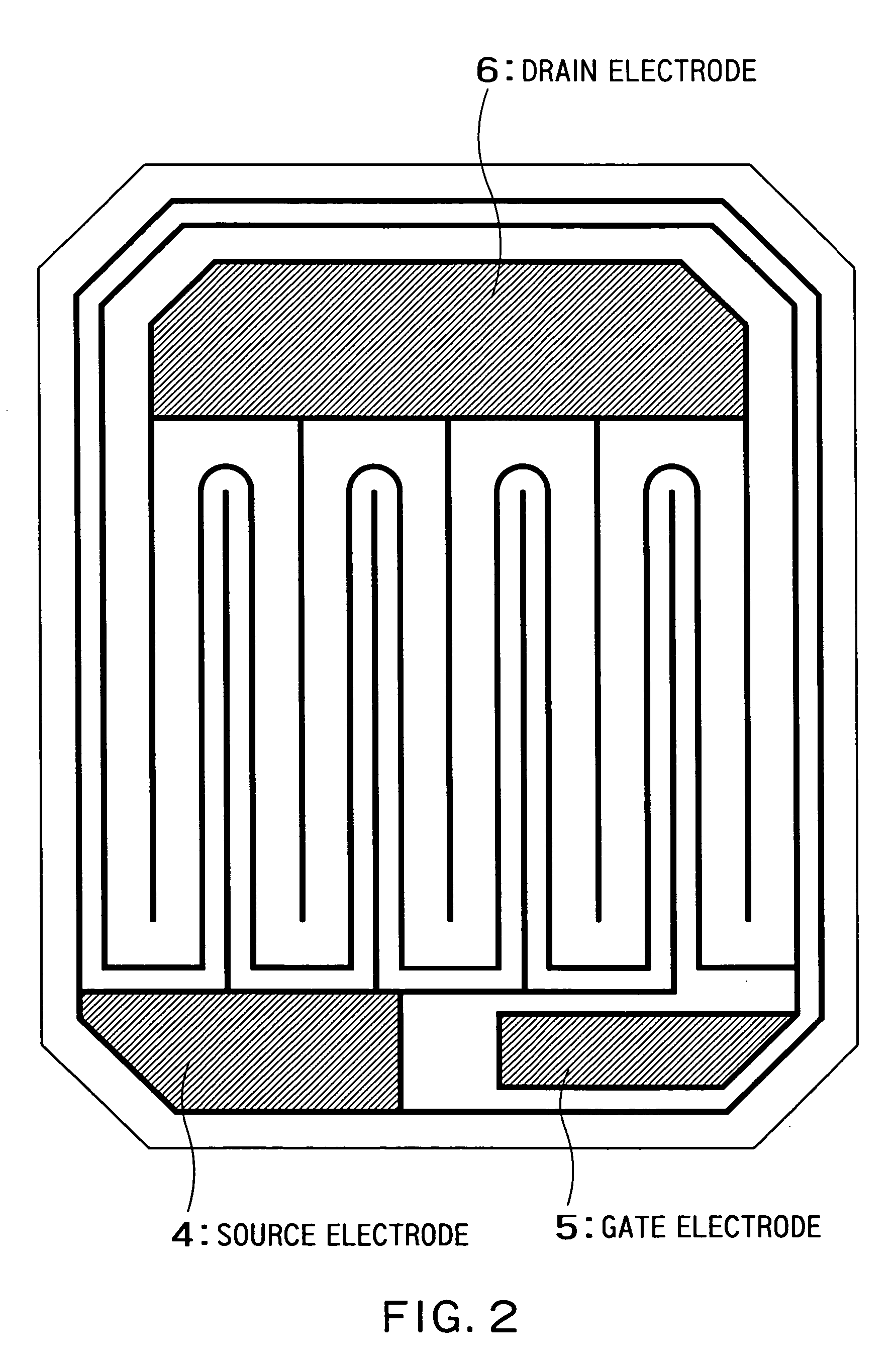
[0050]FIG. 2 is a plan view schematically showing a structure of a nitride semiconductor device according to the present invention, and specifically a plan view where the island-shaped nitride semiconductor layer formed on the silicon substrate is viewed from above.

[0051] On the contrary to the nitride semiconductor device according to the first embodiment of the present invention shown in FIG. 1 where the drain electrode 6 is formed on the center portion of the aluminum gallium nitride layer 3, the circular gate electrode 5 is formed around the drain electrode 6, and the circular source electrode 4 is formed around the gate electrode 5, in the nitride semiconductor device according to the second embodiment of the present invention shown in FIG. 2, the source electrode 4, the gate electrode 5, and the drain electrode 6 are formed in the belt shape instead of in the circular shape.

[0052] The nitride semiconductor device according to the second embodiment of the present invention is ...

third embodiment

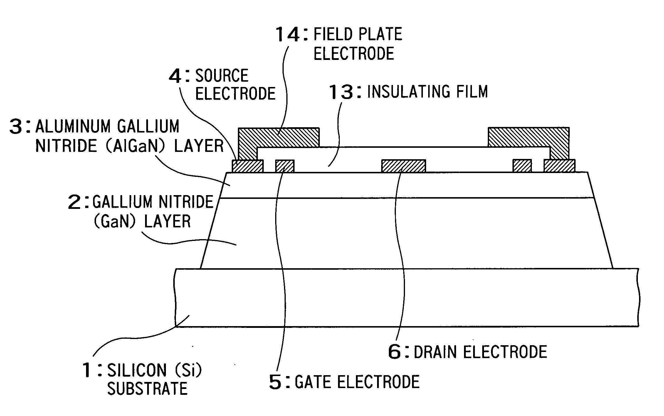
[0061]FIG. 4 is a sectional view showing a structure of a nitride semiconductor device according to the present invention.

[0062] The nitride semiconductor device according to the third embodiment of the present invention is constructed so that additional constituents are added to the nitride semiconductor device according to the first embodiment of the present invention shown in FIG. 1, and comprises a silicon (Si) substrate 1, a gallium nitride (GaN) layer 2 as a first aluminum gallium nitride (AlxGa1-xN (0≦x≦1)) layer formed on the silicon substrate 1 in an island shape, an aluminum gallium nitride (AlGaN) layer 3 as a second aluminum gallium nitride (AlyGa1-yN (0≦y≦1, x2, a drain electrode 6 formed on the center portion of the aluminum gallium nitride layer 3, a gate electrode 5 having a circular shape formed around the drain electrode 6 on the aluminum gallium nitride layer 3, a source electrode 4 having a circular shape formed around the gate electrode 5 on the aluminum gallium...


PUM

PropertyMeasurementUnit
diameteraaaaaaaaaa
thicknessaaaaaaaaaa
breakdown voltageaaaaaaaaaa

Abstract

The nitride semiconductor device according to one embodiment of the present invention comprises: a silicon substrate; a first aluminum gallium nitride (AlxGa1-xN (0≦x≦1)) layer formed as a channel layer on the silicon substrate in an island shape; and a second aluminum gallium nitride (AlyGa1-yN (0≦y≦1, x≦y)) layer formed as a barrier layer of a first conductive type or i-type on the first aluminum gallium nitride layer.

Description

CROSS REFERENCE TO RELATED APPLICATION [0001] The subject application is related to subject matter disclosed in Japanese Patent Application No. 2004-177151 filed on Jun. 15, 2004 in Japan to which the subject application claims priority under Paris Convention and which is incorporated herein by reference. BACKGROUND OF THE INVENTION [0002] 1. Field of the Invention [0003] The present invention relates to a semiconductor device used for power control, and particularly to a nitride semiconductor device such as nitride semiconductor field effect transistor or Schottky barrier diode. [0004] 2. Related Background Art [0005] A nitride semiconductor device where gallium nitride (GaN) is used as part of materials has a larger band gap and a higher critical field as compared with a semiconductor device which does not contain gallium nitride and uses silicon (Si) as main material so that the device having a small size and a high breakdown voltage can be easily achieved. Thus, it is possible t...

Claims


Application Information

Patent Timeline
Patent Type & Authority Applications(United States)
IPC IPC(8): H01L27/06H01L29/20H01L29/40H01L29/417H01L29/778H01L31/109
CPCH01L27/0605H01L24/48H01L29/402H01L29/404H01L29/41725H01L29/7787H01L29/872H01L24/06H01L24/49H01L2224/48091H01L2224/48247H01L2224/48257H01L2224/48472H01L29/2003H01L2924/00014H01L2224/45099H01L2224/45015H01L2924/207H01L2924/00
Inventor SAITO, WATARUOMURA, ICHIRO
Owner KK TOSHIBA
Why Eureka
Try Eureka